Film-forming method for forming passivation film and manufacturing method for solar cell element

Active Publication Date: 2011-12-01
ULVAC INC
View PDF4 Cites 2 Cited by
  • Summary
  • Abstract
  • Description
  • Claims
  • Application Information

AI Technical Summary

Benefits of technology

[0012]According to the film-forming device for forming a passivation film and the film-forming method for forming a passivation film in the present invention, the film quality of the resulting passivation film is satisfactory, and the loss of carriers due to their recombination in a solar cell element can be inhibited. Thus, the excellent effect of improving output characteristics can be exhibited. According to the manufacturing method for a solar cell element of the present invention, the film quality of the passivation film is satisfactory, so that the loss of carriers due to their recombination can be inhibited. This produces the excellent effect of improving output characteristics.

Problems solved by technology

The causes of the loss in the output characteristics of the solar cell element include optical losses, for example, a reflection loss and a transmission loss, and electrical losses, for example, the loss of carriers due to their recombination and an ohmic loss.

Method used


Image

  • Film-forming method for forming passivation film and manufacturing method for solar cell element
  • Film-forming method for forming passivation film and manufacturing method for solar cell element
  • Film-forming method for forming passivation film and manufacturing method for solar cell element

Examples


example 1

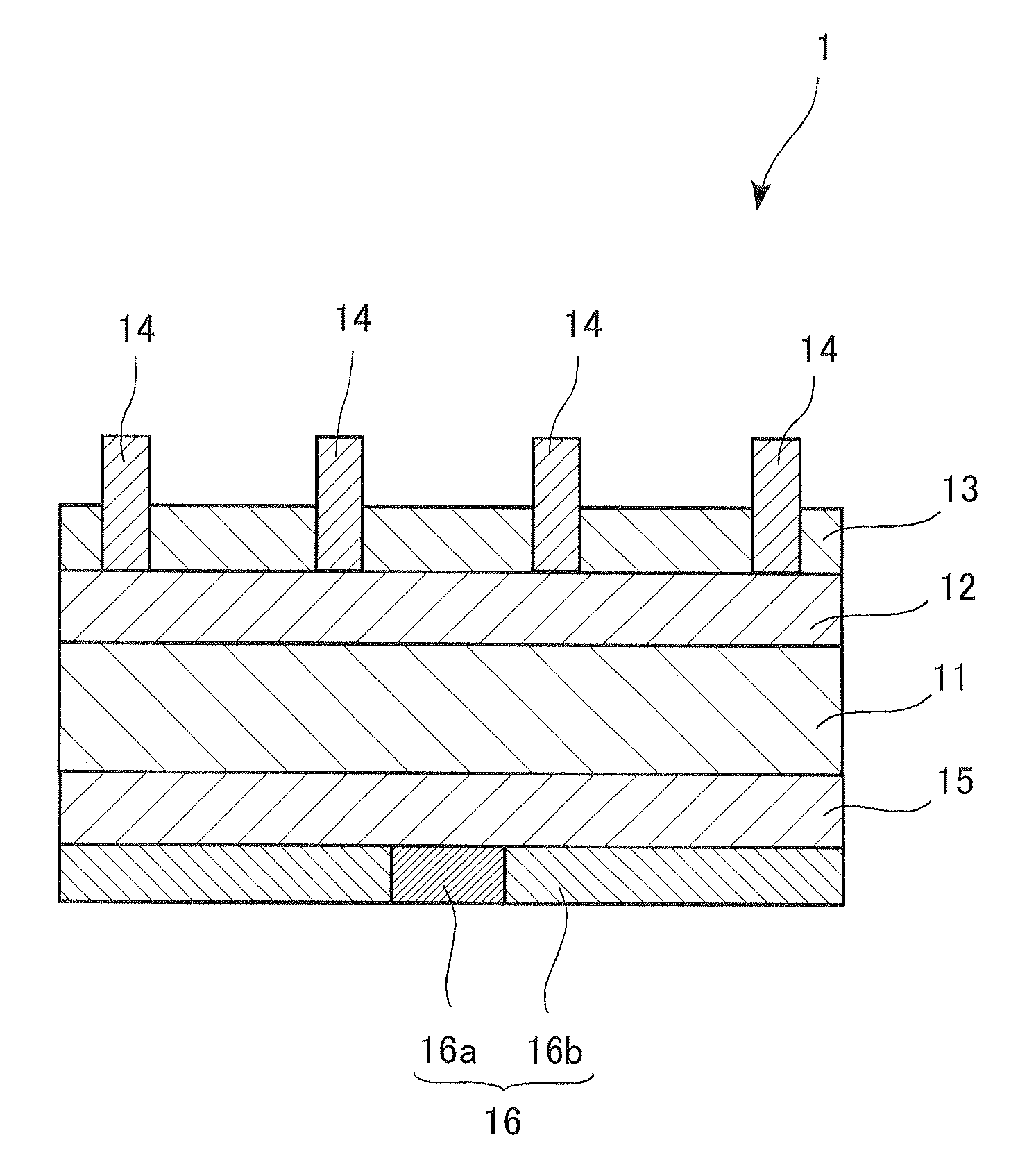
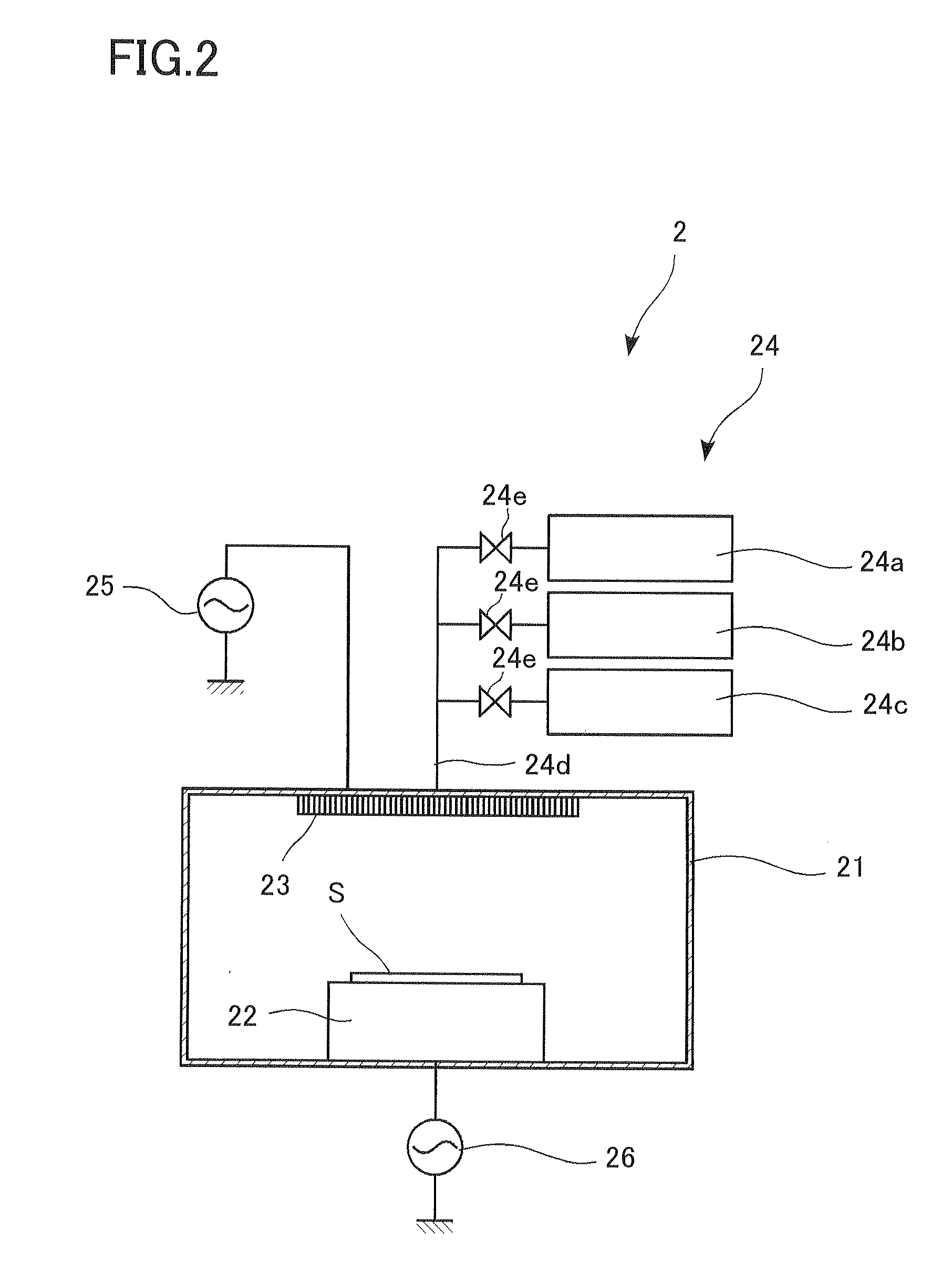
[0039]In the present example, a passivation film was formed using the film-forming device 2 shown in FIG. 2, whereafter a solar cell element was prepared.

[0040]First, an n-type diffusion layer 12 was formed on a surface of a 220 μm thick p-type semiconductor substrate 11 (156 mm×156 mm) of monocrystal silicon having irregularities provided on the surface by texture etching. A plurality of the so treated substrates 11 were arranged side by side on a tray to provide a film-forming object S.

[0041]Then, the film-forming object S was carried into the film-forming device 2 shown in FIG. 2, and a passivation film comprising a silicon nitride film was formed under the following conditions: Substrate temperature: 350° C., SiH4 flow rate: 1500 sccm, NH3 flow rate: 5000 sccm, N2 flow rate: 6000 sccm, frequency of the high frequency power source 25: 13.56 MHz, inputting power of the high frequency power source 25: 1500 W, pressure within the vacuum chamber: 100 Pa, E / S: 14 mm, frequency of the ...

example 2

[0044]In the present example, a solar cell element 1 was produced under exactly the same conditions as those in Example 1, except that the inputting power of the low frequency power source 26 was set at 1000 W.

example 3

[0045]In the present example, a solar cell element 1 was produced under exactly the same conditions as those in Example 1, except that a passivation film was formed using the film-forming device 3 shown in FIG. 3.


PUM

PropertyMeasurementUnit
Fractionaaaaaaaaaa
Frequencyaaaaaaaaaa
Frequencyaaaaaaaaaa

Abstract

The challenge for the present invention is to provide a film-forming method and for forming a passivation film which can sufficiently inhibit the loss of carriers due to their recombination; and a method for manufacturing a solar cell element with the use of the method or the device. The film-forming device comprises a mounting portion 22 for mounting a film-forming object, a high frequency power source 25, and a shower plate 23 which is provided to face the film-forming object S mounted on the mounting portion 22, which introduces a film-forming gas, and to which the high frequency power source is connected and a high frequency voltage is applied. A low frequency power source 26 for applying a low frequency voltage is connected to the shower plate or the mounting portion mounting a substrate. The film-forming method is performed using the film-forming device, and the film-forming method is carried out in forming a passivation film.

Description

CROSS-REFERENCED TO RELATED APPLICATION[0001]This application is a National Stage entry of International Application No. PCT / JP2009 / 071767, filed on Dec. 28, 2009, which claims priority to Japanese Patent Application 2008-335051, filed Dec. 26, 2008. The disclosure of the prior application is hereby incorporated in its entirety by reference.TECHNICAL FIELD[0002]This invention relates to a film-forming for a passivation film, and a manufacturing method for a solar cell element.BACKGROUND ART[0003]A solar cell element, attracting attention as a clean source of energy, is required to reduce a loss in output characteristics for increased output characteristics. The causes of the loss in the output characteristics of the solar cell element include optical losses, for example, a reflection loss and a transmission loss, and electrical losses, for example, the loss of carriers due to their recombination and an ohmic loss.[0004]Patent Document 1, for example, discloses a solar cell element e...

Claims


Application Information

Patent Timeline
IPC IPC(8): H01L31/18
CPCC23C16/5096H01L31/02167H01L31/022425Y02E10/547H01L31/1804H01L31/1868H01L31/18Y02P70/50H01L31/0216H01L31/04
Inventor KUBO, MASASHIKIKUCHI, MAKOTOSAITO, KAZUYAWATAI, MIWASHIMIZU, MIHO
Owner ULVAC INC
Why Eureka
Try Eureka