Gate electrodes for millimeter-wave operation and methods of fabrication

a technology of millimeter-wave operation and gate electrode, which is applied in the direction of semiconductor devices, basic electric elements, electrical equipment, etc., can solve the problems of affecting device operation, gaps may form between the edges of the dielectric and the gate electrode, and more familiar semiconductor materials may not be well-suited for high power and/or high frequency applications

Active Publication Date: 2010-11-04
WOLFSPEED INC
View PDF60 Cites 31 Cited by
  • Summary
  • Abstract
  • Description
  • Claims
  • Application Information

AI Technical Summary

Problems solved by technology

However, these more familiar semiconductor materials may not be well-suited for high power and / or high frequency applications, for example, due to their relatively small bandgaps (1.12 eV for Si and 1.42 for GaAs at room temperature) and relatively small breakdown voltages.
However, in such conventional methods, gaps may be formed between the edges of the dielectric and the gate electrode, due to isotropy of the dielectric etch.
This may be detrimental to device operation, as the unpassivated semiconductor surface exposed by the gap may cause current collapse and / or drift in the device.
In addition, although a passivation layer may be formed in the gap after formation of the gate, the passivation properties of such a post-gate passivation layer may be inferior to that of the initial pre-gate dielectric.
This may be due to the fact that the pre-gate dielectric can be formed at relatively high temperatures, which may not be feasible once the gate metallization has been deposited.

Method used


Image

  • Gate electrodes for millimeter-wave operation and methods of fabrication
  • Gate electrodes for millimeter-wave operation and methods of fabrication
  • Gate electrodes for millimeter-wave operation and methods of fabrication

Examples


Embodiment Construction

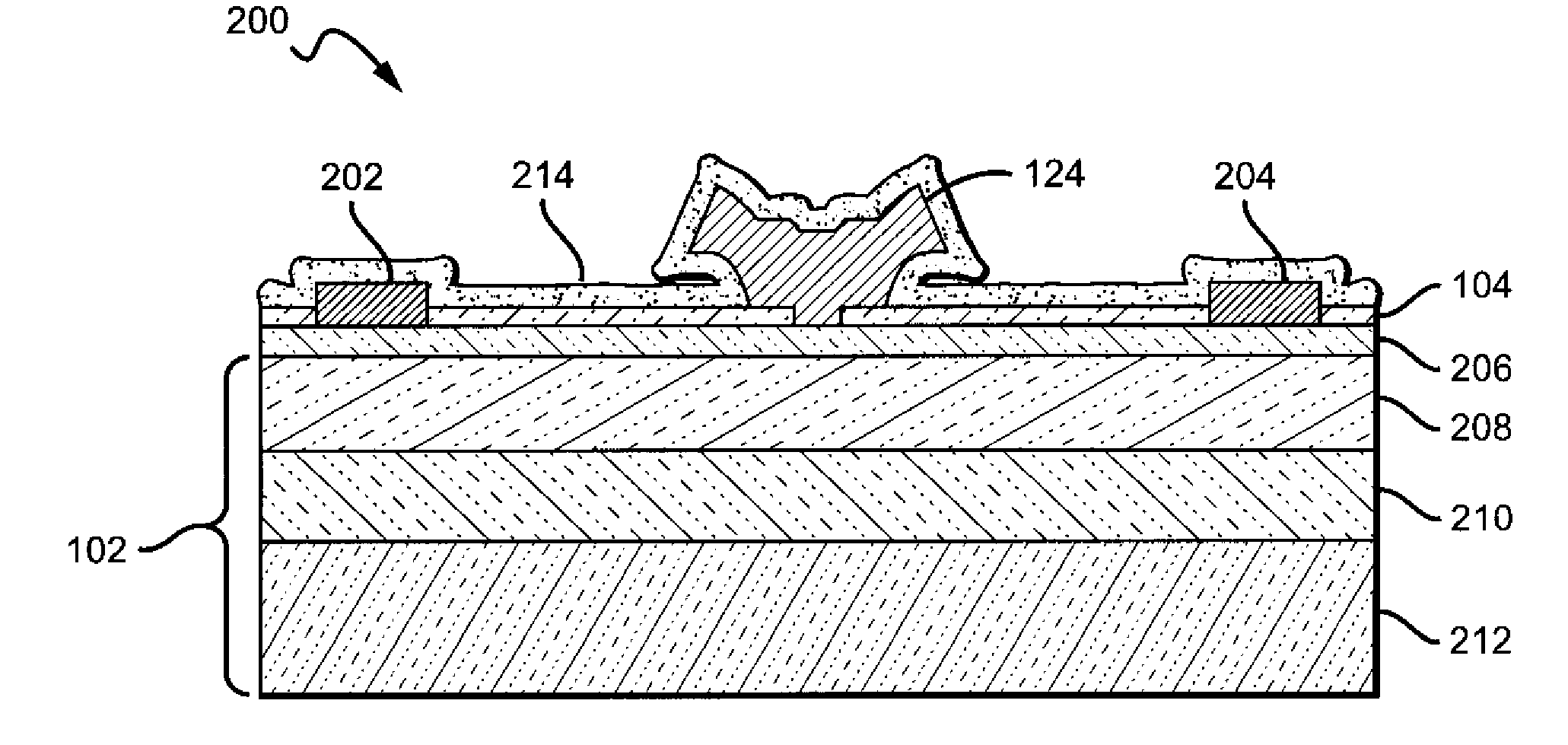
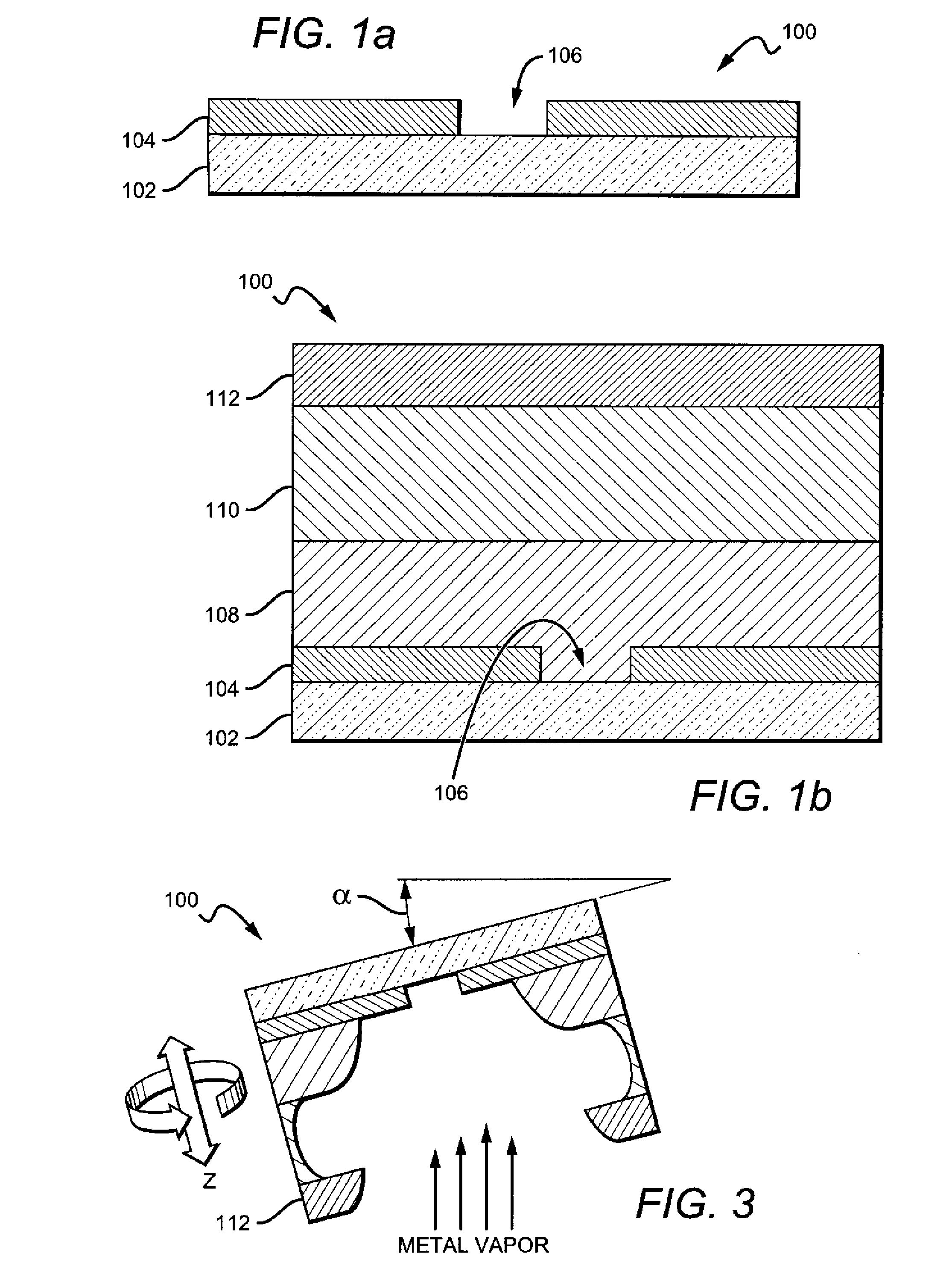
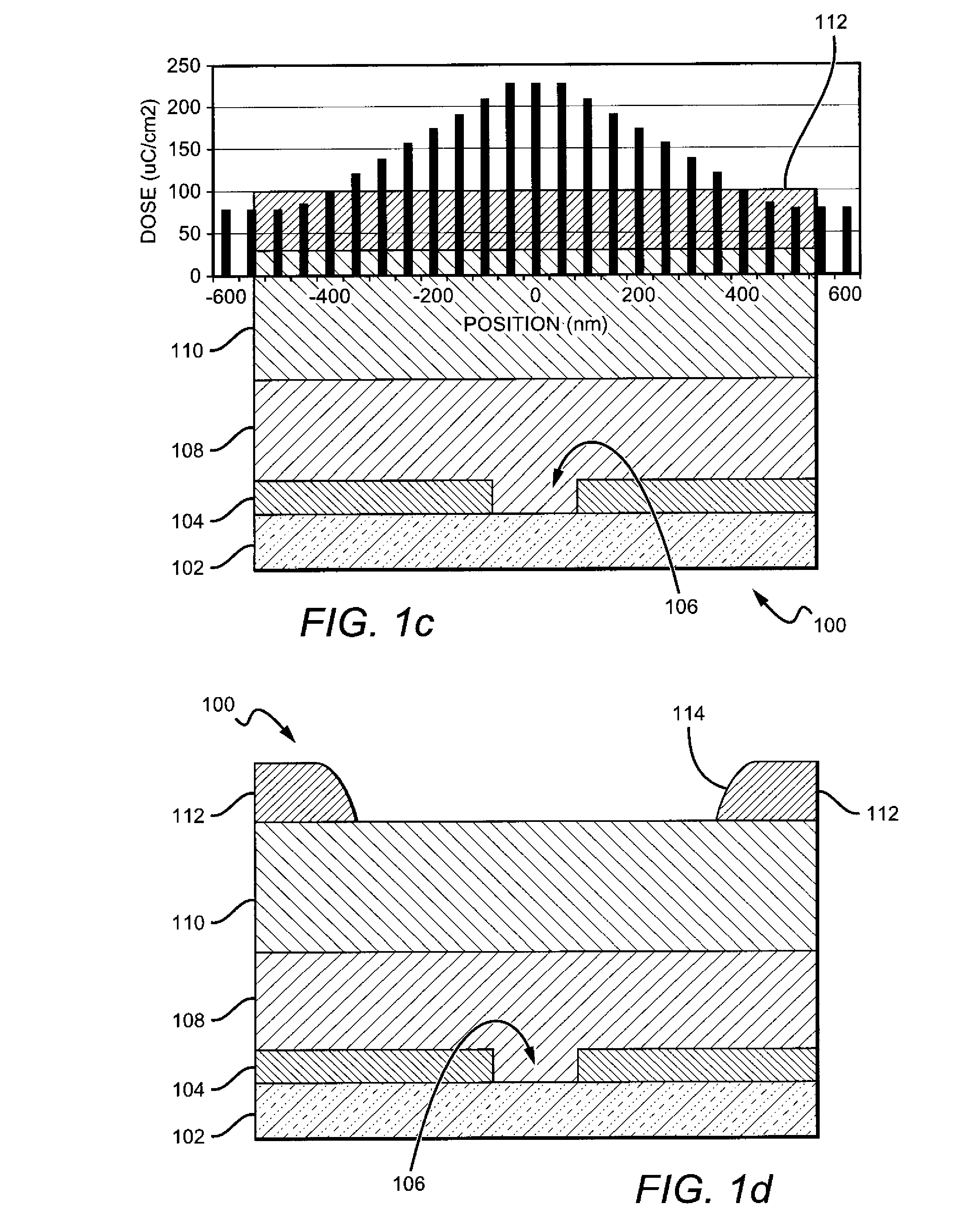
[0020]The present invention is described more fully hereinafter with reference to the accompanying drawings, in which embodiments of the invention are shown. However, this invention should not be construed as limited to the embodiments set forth herein. Rather, these embodiments are provided so that this disclosure is thorough and complete and fully conveys the scope of the invention to those skilled in the art. In the drawings, the thickness of layers and regions are exaggerated for clarity. Like numbers refer to like elements throughout.

[0021]It is understood that when an element such as a layer, region or substrate is referred to as being “on” or extending “onto” another element, it can be directly on or extend directly onto the other element or intervening elements may be present. In contrast, when an element is referred to as being “directly on” or extending “directly onto” another element, there are no intervening elements present. It is also understood that when an element is...


PUM


Abstract

A transistor device having a tiered gate electrode fabricated with methods using a triple layer resist structure. The triple layer resist stack is deposited on a semiconductor structure. An exposure pattern is written onto the resist stack using an e-beam writer, for example. The exposure dose is non-uniform across the device. Portions of the three resist layers are removed with a sequential development process, resulting in tiered resist structure. A conductive material is deposited to form the gate electrode. The resulting “Air-T” gate also has a three-tiered structure. The fabrication process is well-suited for the production of gates small enough for use in millimeter wave devices.

Description

[0001]This invention was made with Government support under Office of Naval Research Contract Nos. N00014-06-C-0156, N00014-03-C-0092, and N00173-07-C-4012. The Government has certain rights in this invention.BACKGROUND OF THE INVENTION[0002]1. Field of the Invention[0003]Embodiments of the invention relate generally to transistors and methods of manufacture and, more particularly, to gate structures for use in transistors and methods of manufacture.[0004]2. Description of the Related Art[0005]Materials such as silicon (Si) and gallium arsenide (GaAs) have found wide application in semiconductor devices for low power and, in the case of Si, low frequency applications. However, these more familiar semiconductor materials may not be well-suited for high power and / or high frequency applications, for example, due to their relatively small bandgaps (1.12 eV for Si and 1.42 for GaAs at room temperature) and relatively small breakdown voltages.[0006]In light of the difficulties presented b...

Claims


Application Information

Patent Timeline
Patent Type & Authority Applications(United States)
IPC IPC(8): H01L29/20H01L21/283H01L21/302
CPCH01L21/0272H01L29/66462H01L21/28587
Inventor MOORE, MARCIAHEIKMAN, STEN
Owner WOLFSPEED INC
Why Eureka
Try Eureka