Active matrix substrate and liquid crystal display device
- Summary
- Abstract
- Description
- Claims
- Application Information
AI Technical Summary
Benefits of technology
Problems solved by technology
Method used
Image

Examples
first embodiment
of the Invention
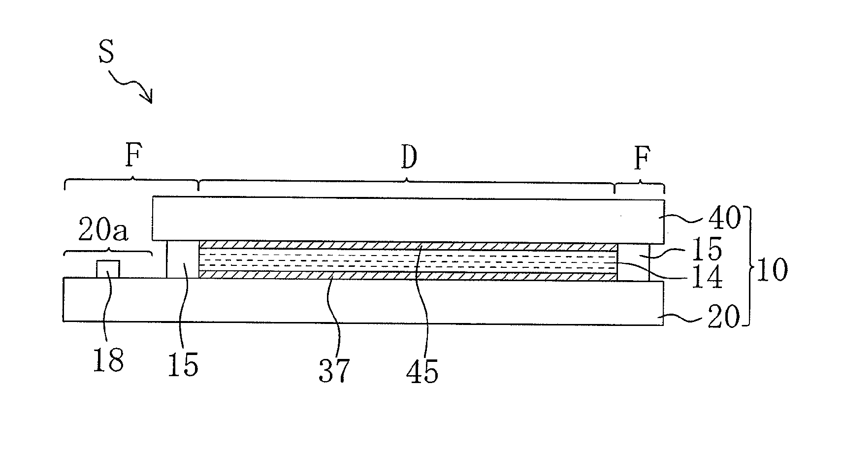
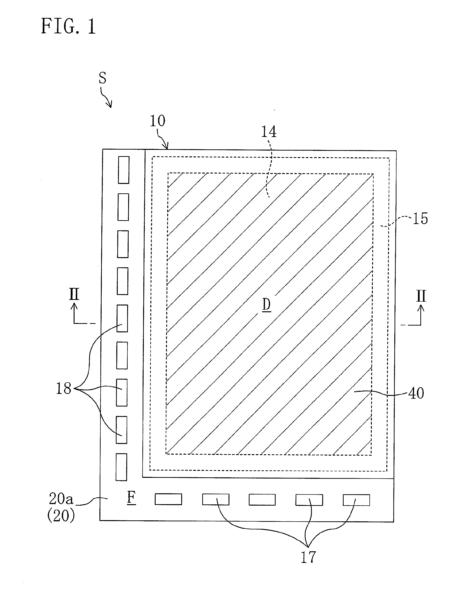
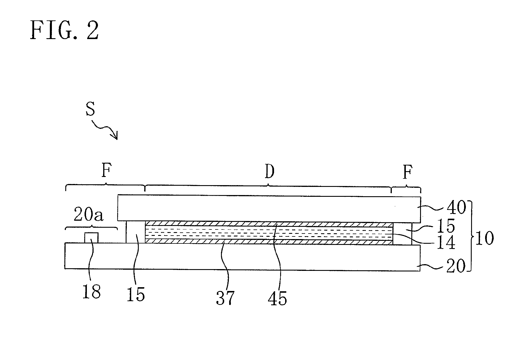
[0056]FIGS. 1 to 8 show a first embodiment of the invention. FIG. 1 is a plan view schematically showing a liquid crystal display device S. FIG. 2 is a cross-sectional view schematically showing the liquid crystal display device S, taken along the line II-II of FIG. 1. FIG. 3 is a plan view schematically showing, on an enlarged scale, part of the liquid crystal display device S. FIG. 4 is a plan view schematically showing, on an enlarged scale, part of one substrate 20 included in the liquid crystal display device S. FIG. 5 is a cross-sectional view schematically showing the liquid crystal display device S, taken along the line V-V of FIG. 3. Note that, in FIG. 4, a laminated insulating film 35 and pixel electrodes 36 are shown transparent.
[0057]The liquid crystal display device S, as shown in FIG. 1 and FIG. 2, includes a liquid crystal display panel 10 in which a pair of substrates 20 and 40 are bonded together. The liquid crystal display panel 10 includes the acti...
second embodiment
of The Invention
[0089]FIGS. 9 to 11 show the second embodiment of the invention. Note that, in the following embodiments, the same parts as those in FIGS. 1 to 8 are denoted by the same reference characters, and the detailed description thereof is omitted. FIG. 9 is a plan view schematically showing one pixel group 12 of the liquid crystal display device S of the present embodiment. FIG. 10 is a plan view schematically showing one pixel region group 23 of the active matrix substrate 20 of the present embodiment. FIG. 11 is a cross-sectional view schematically showing the liquid crystal display device S, taken along the line XI-XI of FIG. 9.
[0090]The liquid crystal display device S of the present embodiment is a liquid crystal display device of what is called MVA (multidomain vertical alignment) method. The liquid crystal layer 14 is made of a vertical alignment type nematic liquid crystal material having a negative dielectric anisotropy, and each of the alignment layers 37 and 45 is...
third embodiment
of the Invention
[0102]FIG. 12 shows the third embodiment of the invention. FIG. 12 is a plan view schematically showing one pixel region group 23 of the active matrix substrate 20 of the present embodiment.
[0103]The liquid crystal display device S in the present third embodiment, as in the above the second embodiment, is an MVA liquid crystal display device. In the auxiliary capacitance electrode 33 of each pixel region 22, a side end on one side in the direction in which the drain electrode 32 crosses the end of the gate electrode 28 so as to enter from the outside of the gate electrode 28 to the inside thereof is disposed inside of the auxiliary capacitance line 26, and a side end on the other side in the direction in which the drain electrode 32 crosses the end of the gate electrode 28 so as to go out from the inside of the gate electrode 28 to the outside thereof is disposed outside of the auxiliary capacitance line 26.
[0104]In the above second embodiment, in each auxiliary capa...
PUM
 Abstract
Description
Claims
Application Information
 - Generate Ideas
- Intellectual Property
- Life Sciences
- Materials
- Tech Scout
- Unparalleled Data Quality
- Higher Quality Content
- 60% Fewer Hallucinations
Browse by: Latest US Patents, China's latest patents, Technical Efficacy Thesaurus, Application Domain, Technology Topic, Popular Technical Reports.
© 2025 PatSnap. All rights reserved.Legal|Privacy policy|Modern Slavery Act Transparency Statement|Sitemap|About US| Contact US: help@patsnap.com