Integrated solar cell nanoarray layers and light concentrating device

a solar cell and nanoarray technology, applied in semiconductor devices, instruments, electrical devices, etc., can solve the problems of not being able to solve the problem of light coupling directly from the incident surface, not being able to solve the problem of 105/b>current generation in the material layer, and achieving a far less efficient process

Inactive Publication Date: 2010-11-18
LIGHTWAVE POWER
View PDF9 Cites 55 Cited by
  • Summary
  • Abstract
  • Description
  • Claims
  • Application Information

AI Technical Summary

Problems solved by technology

However, the use of thin layers limits absorption and therefore the current generated in material layer 105 is limited.
Unfortunately, by Snell's law of classical optics, there is not a solution where light can be coupled directly from an incident surface into total internal reflection m...

Method used


Image

  • Integrated solar cell nanoarray layers and light concentrating device
  • Integrated solar cell nanoarray layers and light concentrating device
  • Integrated solar cell nanoarray layers and light concentrating device

Examples


Embodiment Construction

Definitions

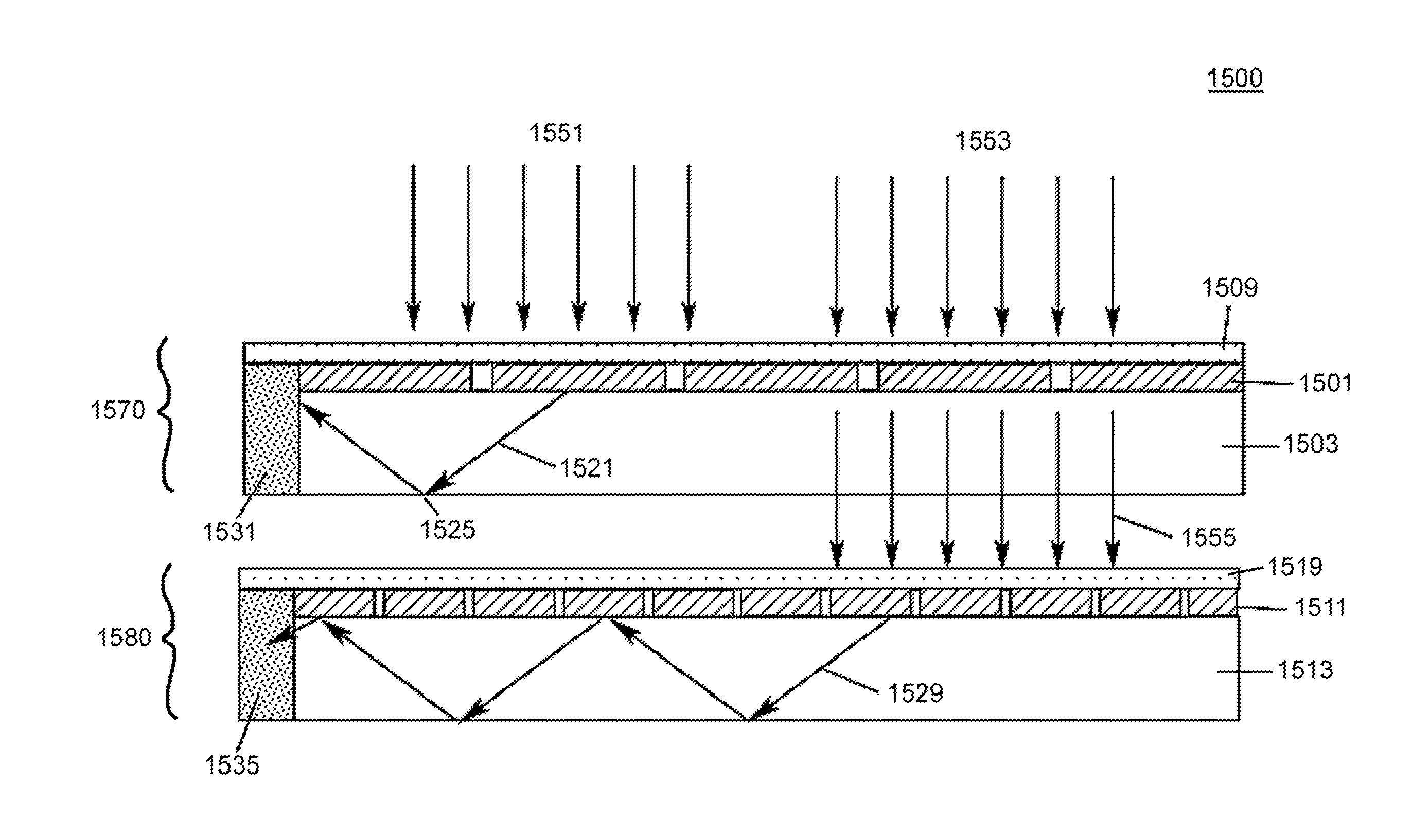
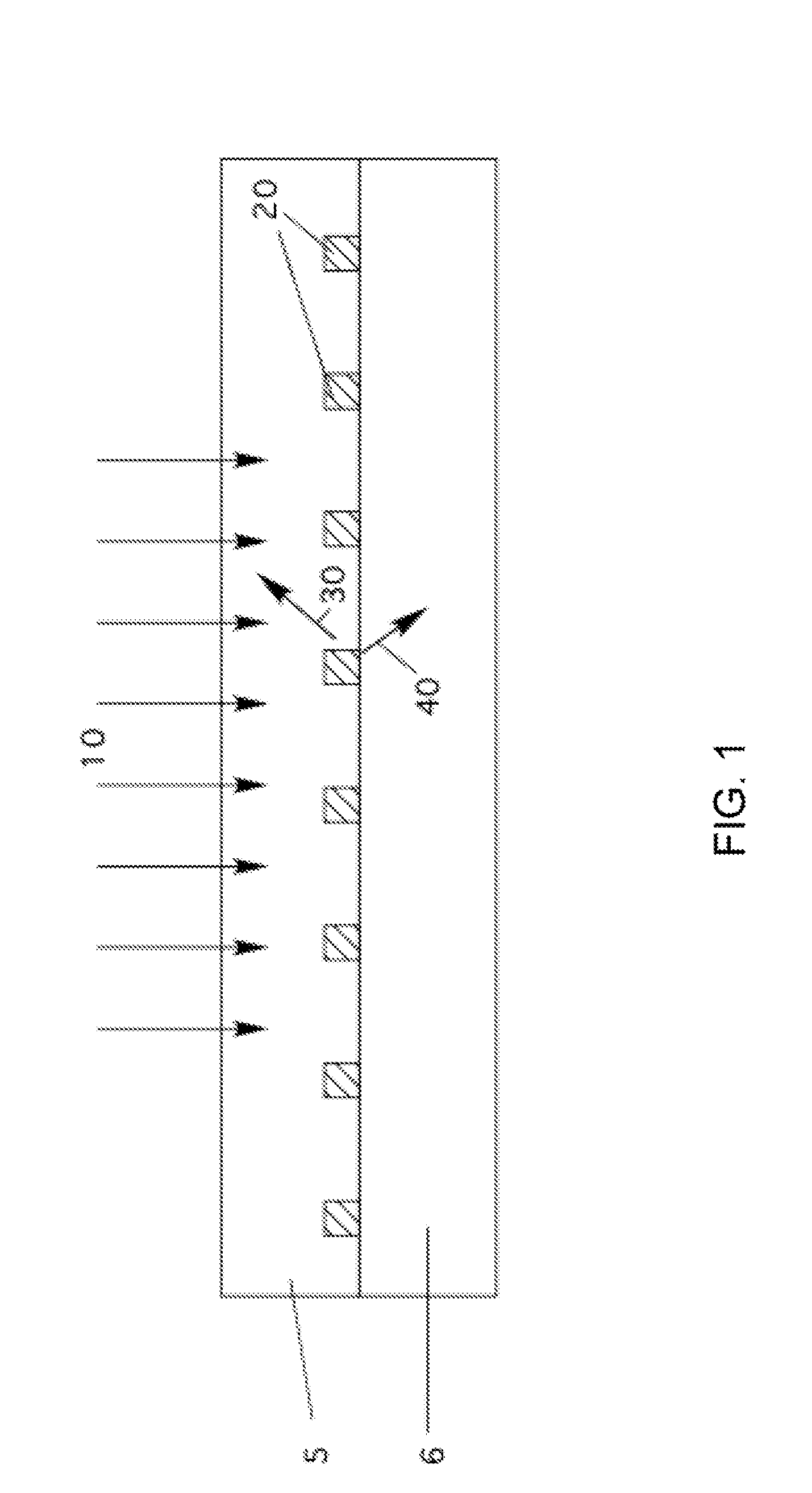
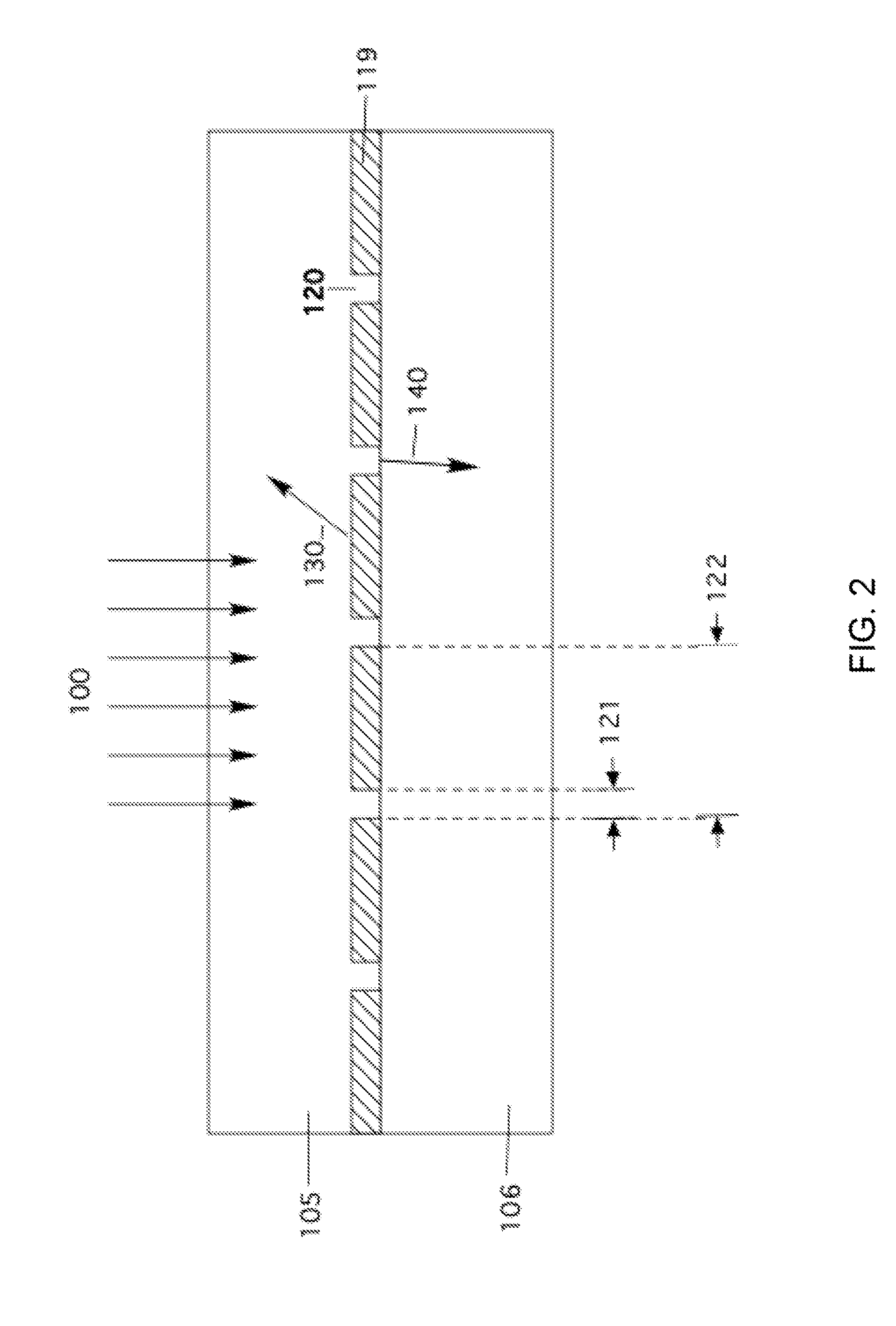
[0047]Integrated solar cell: We refer herein to a complete solar cell assembly of layers as an “integrated solar cell”. The term integrated solar cell, includes integrated structures made using both conventional semiconductor manufacturing methods, e.g. photolithography and vapor deposition, as well as layers manufactured in part or entirely by more recent fabrication methods, such as for example, nanofabrication methods.

[0048]Solar cell layer: The absorber of an integrated solar cell is referred to interchangeably herein as a “solar cell layer”. It is understood that one or more solar cell layers are electrically coupled within an integrated solar cell to provide an integrated solar cell electrical output voltage across an integrated solar cell positive terminal and an integrated solar cell negative terminal. In some embodiments a metal film present for optical reasons can also, but not necessarily, provide as an electrical connection to a solar cell layer.

[0049]Nanoarra...


PUM


Abstract

An integrated energy conversion device includes a nanoarray layer having a plurality of nanofeatures disposed in a pattern. The nanoarray layer is configured to modify a selected one of a direction and a wavelength of photons of light incident on a surface of the nanoarray layer. The nanoarray layer has a surface. A first material is disposed adjacent to and optically coupled to one region of the surface of the nanoarray layer. A second material is disposed adjacent to and optically coupled to a second region of the surface of the nanoarray layer. At least a selected one of the first material and the second material includes a photovoltaic layer which is configured to provide an integrated solar cell electrical output voltage and an integrated solar cell electrical output current between an integrated solar cell positive output terminal and an integrated solar cell negative output terminal.

Description

CROSS-REFERENCE TO RELATED APPLICATIONS[0001]This application claims priority to and the benefit of co-pending U.S. provisional patent application Ser. No. 61 / 177,449, PATTERNED PLANAR DEVICES AS INTERMEDIATE LIGHT DISTRIBUTING AND GUIDING LAYERS IN SOLAR CELLS, filed May 12, 2009, and co-pending U.S. provisional patent application Ser. No. 61 / 177,462, PLASMONIC AND PHOTONIC STRUCTURES FOR GUIDING AND TRAPPING LIGHT, filed May 12, 2009 which applications are incorporated herein by reference in their entirety.FIELD OF THE INVENTION[0002]The invention relates to light management layers in general and particularly to light management device layers that employ nanoarrays.BACKGROUND OF THE INVENTION[0003]Integrated solar cells include at least one solar cell or absorbing layer which absorbs photons of light for conversion to electricity. One problem with integrated solar cells is that conventional solar cell layers are relatively thick. The present use of relatively thick solar cell laye...

Claims


Application Information

Patent Timeline
IPC IPC(8): H01L31/0232
CPCH01L31/0549G02B2207/101Y02E10/544H01L31/02168H01L31/0547H01L31/0687Y02E10/52G02B5/008H01L31/055Y02E10/546
Inventor JI, JINKAUFMAN, LAWRENCE
Owner LIGHTWAVE POWER
Why Eureka
Try Eureka