
Prism coupled silicon on insulator sensor

a technology of coupled silicon and insulator, which is applied in the direction of phase-affecting property measurement, measurement devices, instruments, etc., can solve the problems of limiting the ultimate sensitivity of spr technique, and inadvisable to work at longer wavelengths

Inactive Publication Date: 2010-11-18
NAT RES COUNCIL OF CANADA
View PDF2 Cites 2 Cited by
  • Summary
  • Abstract
  • Description
  • Claims
  • Application Information

AI Technical Summary

Problems solved by technology

While useful, SPR has its drawbacks.
This, unfortunately, limits the ultimate sensitivity of the SPR technique.
Working at longer wavelengths is, therefore, inadvisable for the SPR technique.

Method used


Image

  • Prism coupled silicon on insulator sensor
  • Prism coupled silicon on insulator sensor
  • Prism coupled silicon on insulator sensor

Examples


Embodiment Construction

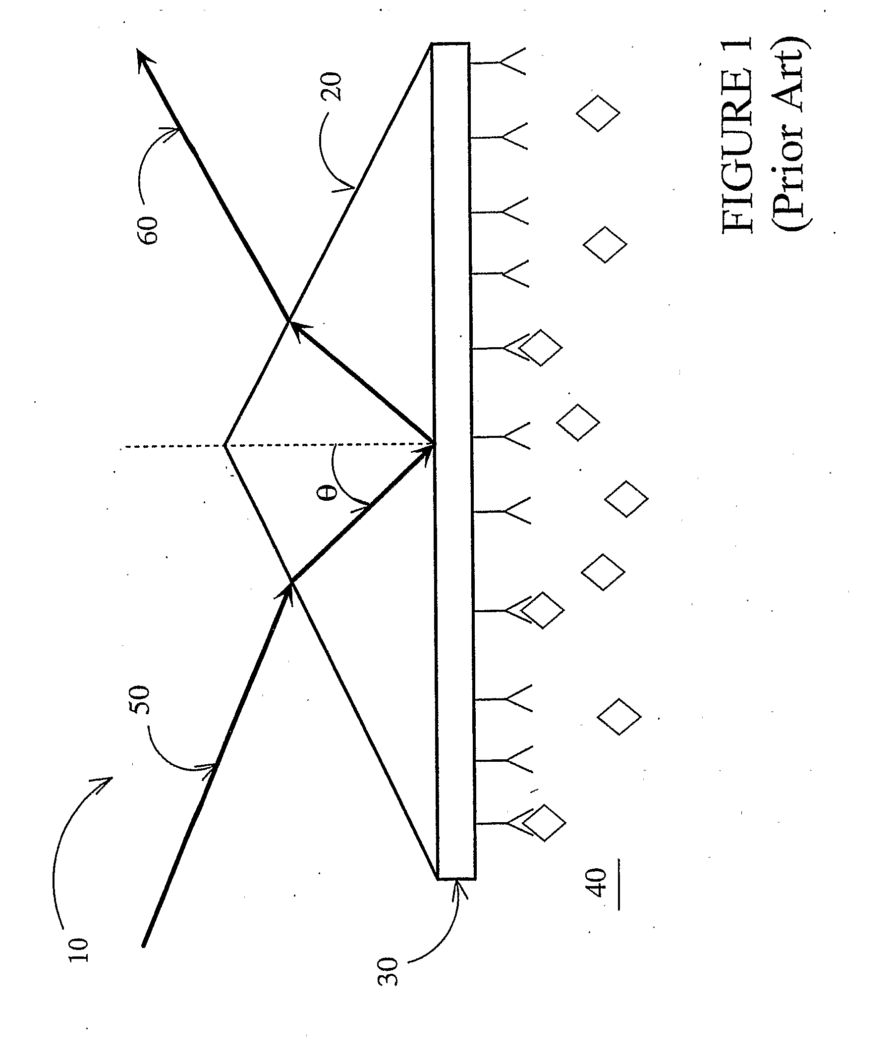
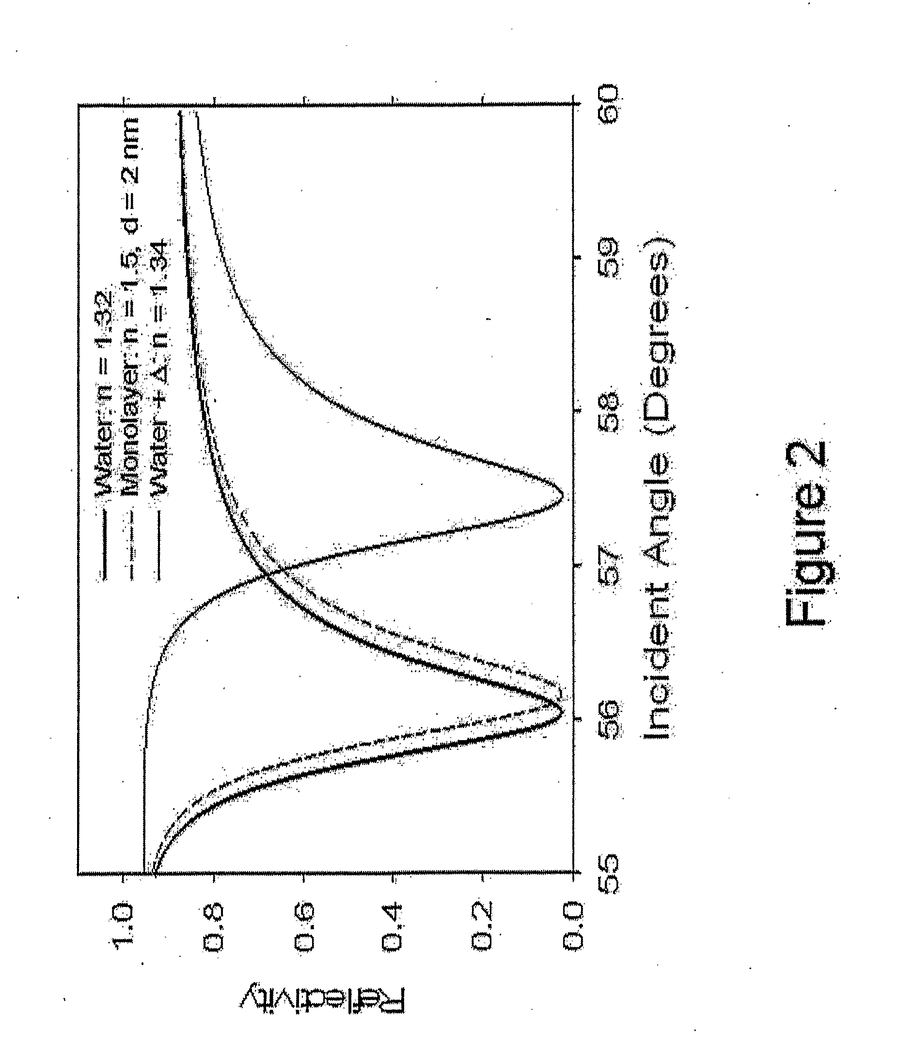
[0035]Referring to FIG. 1, an SPR sensor according to the prior art is illustrated. In the sensor 10, a prism 20 is optically coupled to a gold film 30. Material 40 to be examined (an analyte plus water in one instance) is exposed to the gold film 30. An incident light 50 enters the prism 20 at an incident angle θ and is reflected out of the prism 20 as reflected light 60. As the incident angle θ changes, at some point the incident light couples to the SPR mode in the gold film 30. When this occurs, the intensity of the reflected light 60 significantly drops off. The angle at which this occurs changes as the refractive index of the material 40 immediately adjacent to the metal surface changes. This change in the refractive index of the material 40 is in proportion to the amount of analyte bound to the gold film 30—as the refractive index changes, the incident angle at which coupling occurs changes as well.

[0036]As can be seen from FIG. 2, the decrease in intensity of the reflected l...


PUM

PropertyMeasurementUnit
thicknessaaaaaaaaaa
thicknessaaaaaaaaaa
thicknessaaaaaaaaaa

Abstract

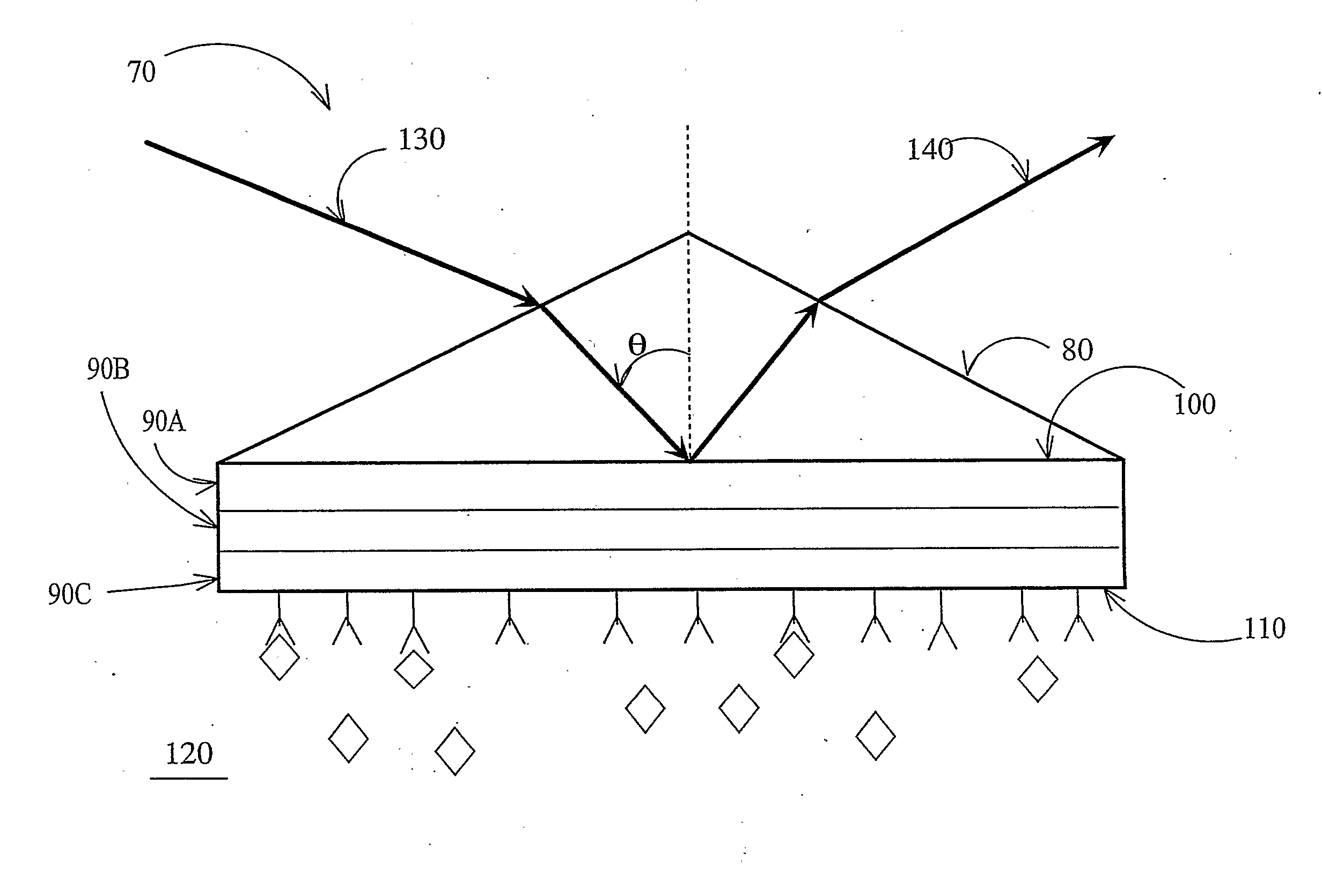
Methods and devices related to a sensor element for use in the detection and monitoring of molecular interactions. The sensor element uses a silicon-on-insulator wafer optically coupled to a silicon prism. The wafer has a thin silicon film top layer, a silicon substrate layer, and a buried silicon dioxide layer sandwiched between the silicon film and substrate layers. The wafer is coupled to the prism on the wafer's substrate side while the interactions to be monitored are placed on the wafer's silicon film side. An incident beam is directed at the prism and the incident angle is adjusted until the beam optically couples to the silicon film's optical waveguide mode. When this occurs, a decrease in the intensity of the reflected beam can be detected. The molecular interactions affect the phase velocity or wave vector of the propagating mode. Similarly, instead of measuring the incident angle at which optical coupling occurs, the phase of the reflected beam may be measured.

Description

FIELD OF THE INVENTION[0001]The present invention relates to sensor equipment for use in detecting and monitoring molecular interactions. More specifically, the present invention relates to a sensor element which uses a silicon-on-insulator wafer along with a silicon prism.BACKGROUND TO THE INVENTION[0002]The field of biological and biochemical research has significantly grown in the past decade. More and more new compounds, medicines, and techniques are being developed in these fields. One key activity for such research is the detection and monitoring of molecular interactions. Molecular binding between compounds are presently detected and monitored using a number of techniques, the most common being SPR (surface plasmon resonance).[0003]SPR is well-known and is, at present, the only label-free sensor technology commercially available for monitoring molecular binding interactions in real time. An SPR system measures the shift in surface plasmon phase velocity or wavevector as the m...

Claims


Application Information

Patent Timeline
Patent Type & Authority Applications(United States)
IPC IPC(8): G01N21/41
CPCG01N21/552
Inventor XU, DAN-XIADENSMORE, ADAMDELAGE, ANDRECHEBEN, PAVELJANZ, SIEGFRIED
Owner NAT RES COUNCIL OF CANADA
Learn More