
Method for Making a Piezoceramic Device

a manufacturing method and ceramic technology, applied in piezoelectric/electrostrictive/magnetostrictive devices, thin material processing, transportation and packaging, etc., can solve the problems of reduced ceramic sensitivity, reduced insulating resistance, and increased dielectrcial losses, so as to achieve reasonable engineering effort and expense, the effect of not oxidizing

Inactive Publication Date: 2010-11-25
EPCOS AG
View PDF13 Cites 3 Cited by
  • Summary
  • Abstract
  • Description
  • Claims
  • Application Information

AI Technical Summary

Benefits of technology

The use of copper electrodes facilitates efficient and cost-effective production of piezoceramic devices with superior quality, maintaining high electromechanical coupling factors and preventing reductive degradation, thus overcoming the limitations of Ag / Pd electrodes.

Problems solved by technology

La2O3—in particular Nd2O3—additives induce the production of cation vacancies in the Pb positions of the crystal structure and at the same time increase the tendency to act as donors, particularly at insufficient oxygen partial pressure, which can lead to a depression of the insulating resistance and a rise in the dielectrcial losses, i.e., the sensitivity of the ceramic towards reduction is increased.
This production method is costly.
Furthermore, these piezoactuators have the disadvantage that the glue used has a negative effect on the electrical characteristics.
However, the disclosed method does not lend itself to the requirements of an efficient production, including foil multilayer technology, and is therefore not appropriate for a mass production.
The process is interference-prone, because of the shrinkage during the reduction from copper oxide to copper and resulting delamination and has up to now not been technologically converted into products.

Method used

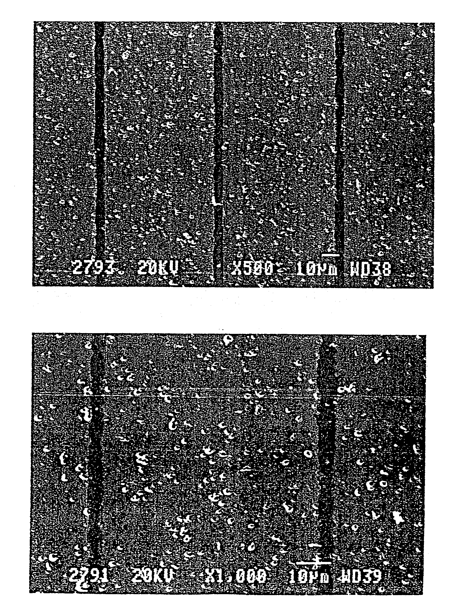

Image

  • Method for Making a Piezoceramic Device
  • Method for Making a Piezoceramic Device
  • Method for Making a Piezoceramic Device

Examples


Embodiment Construction

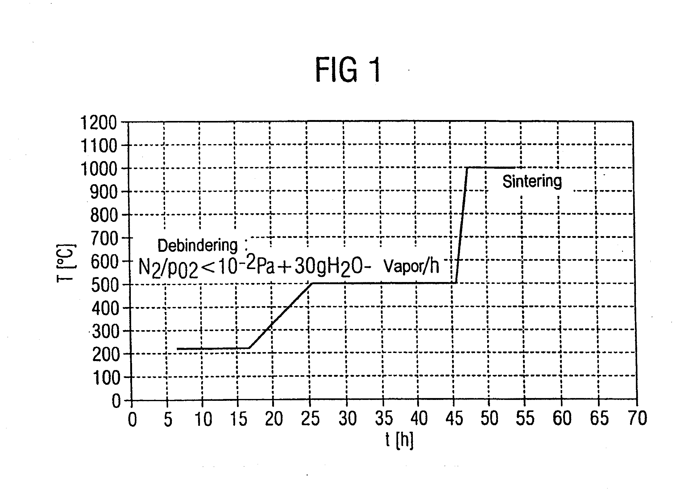
[0032]A piezoceramic Perovskite-mixed crystal phase is built according to the following steps: TiO2, ZrO2 (each may be from a mixed precipitation produced precursor (Zr, Ti)O2) and PbCo3 (e.g., Pb3O4 and dopants like La2O3 or from another oxyde of the rare earth metals) and if necessary an additive of CuO based raw material mixture is set in its composition on the morphotropic phase interface with a PbO-surplus of maximally 5% to support the sinter condensation; for even distribution, the component undergoes a grinding step in diluted suspension and is calcinated after the filtering; and drying occurs at 900 to 950° C. To obtain sinter condensation in 2 to 4 hours at about 1000° below the melting temperature of copper, a pulverization to a medium grain size 96% of the theoretical density at both sufficient grain growth and adequate mechanical solidity in the ceramic structure.

[0033]The finely ground powder is suspended in a diluted slip with approx. 70 m-% solid substance content by...


PUM

PropertyMeasurementUnit
temperatureaaaaaaaaaa
partial pressureaaaaaaaaaa

Abstract

The invention concerns a method for making a piezoelectrical device, whose electrode layers contain copper. The usage of copper in the electrode layers is enabled by a debindering process, which is carried out by steam.

Description

CROSS REFERENCE TO RELATED APPLICATIONS[0001]This application is a divisional of U.S. patent application Ser. No. 11 / 406,587 filed Apr. 19, 2006, now allowed, which is a Continuation of U.S. patent application Ser. No. 09 / 736,266 filed Dec. 15, 2000, Abandoned, which claims priority from German Application No. 199 60 849 filed Dec. 16, 1999.FIELD OF THE INVENTION[0002]The present invention relates to a method for manufacturing a piezoceramic device wherein the device includes a stack of at least two ceramic layers and an electrode layer arranged between two ceramic layers.[0003]Such devices may comprise a plurality of layers and uses. For example, they may be used in: actuators for effecting a low-inertia mechanical vibration of comparably high force via application of a select control voltage; bending elements to effect a high mechanical vibration of less force via application of select control voltage; or production of high electrical voltages. Piezoceramic devices may serve to de...

Claims


Application Information

Patent Timeline
Patent Type & Authority Applications(United States)
IPC IPC(8): C03B29/00C04B35/64C04B35/638C04B37/02H10N30/053H10N30/50H10N30/853H10N30/87
CPCC04B35/493Y10T428/12507C04B37/021C04B2235/3224C04B2235/3227C04B2235/3281C04B2235/5445C04B2235/6562C04B2235/6567C04B2235/6582C04B2235/6584C04B2235/6586C04B2235/6588C04B2235/721C04B2235/77C04B2235/785C04B2235/786H01L41/0471H01L41/0477H01L41/1876H01L41/273C04B2237/407C04B2235/768C04B2237/346C04B2237/348Y10T29/435Y10T428/24926Y10T428/252Y10T29/49117Y10T29/42Y10T29/49005C04B35/638Y10T428/31678H10N30/871H10N30/877H10N30/8554H10N30/053
Inventor FELTZ, ADALBERTGANSBERGER, SIGRIDFLORIAN, HEINZKASTL, HARALD
Owner EPCOS AG
Learn More