Light emitting device

a technology of light emitting device and light source, which is applied in the direction of semiconductor devices for light sources, lighting and heating apparatus, instruments, etc., can solve the problems of non-uniform light or low color rendering index of light sources, increased size of led illumination devices, and user discomfort, and achieves the effect of enhancing the light emitting uniformity of light emitting devices

Inactive Publication Date: 2010-11-25
EVERLIGHT ELECTRONICS
View PDF25 Cites 30 Cited by
  • Summary
  • Abstract
  • Description
  • Claims
  • Application Information

AI Technical Summary

Benefits of technology

[0008]An embodiment of the invention provides a light emitting device, which includes a transparent plate for enhancing the light emitting uniformity of the light emitting device.

Problems solved by technology

In other words, the light beam generated by the LED has high directivity, and thus may result in unfavorable light uniformity and glares that would cause discomfort of the user.
The size of the whole LED illumination device is increased as a consequence, which causes inconvenience.
However, if the optical glass is covered on the LED, then an illumination angle generated by the entire LED illumination module may be too small or focused at a certain region, while even having problems such as non-uniform light or low color render index of the light source.

Method used


Image

  • Light emitting device
  • Light emitting device
  • Light emitting device

Examples


Embodiment Construction

[0065]Reference will now be made in detail to the present preferred embodiments of the invention, examples of which are illustrated in the accompanying drawings. Wherever possible, the same reference numbers are used in the drawings and the description to refer to the same or like parts.

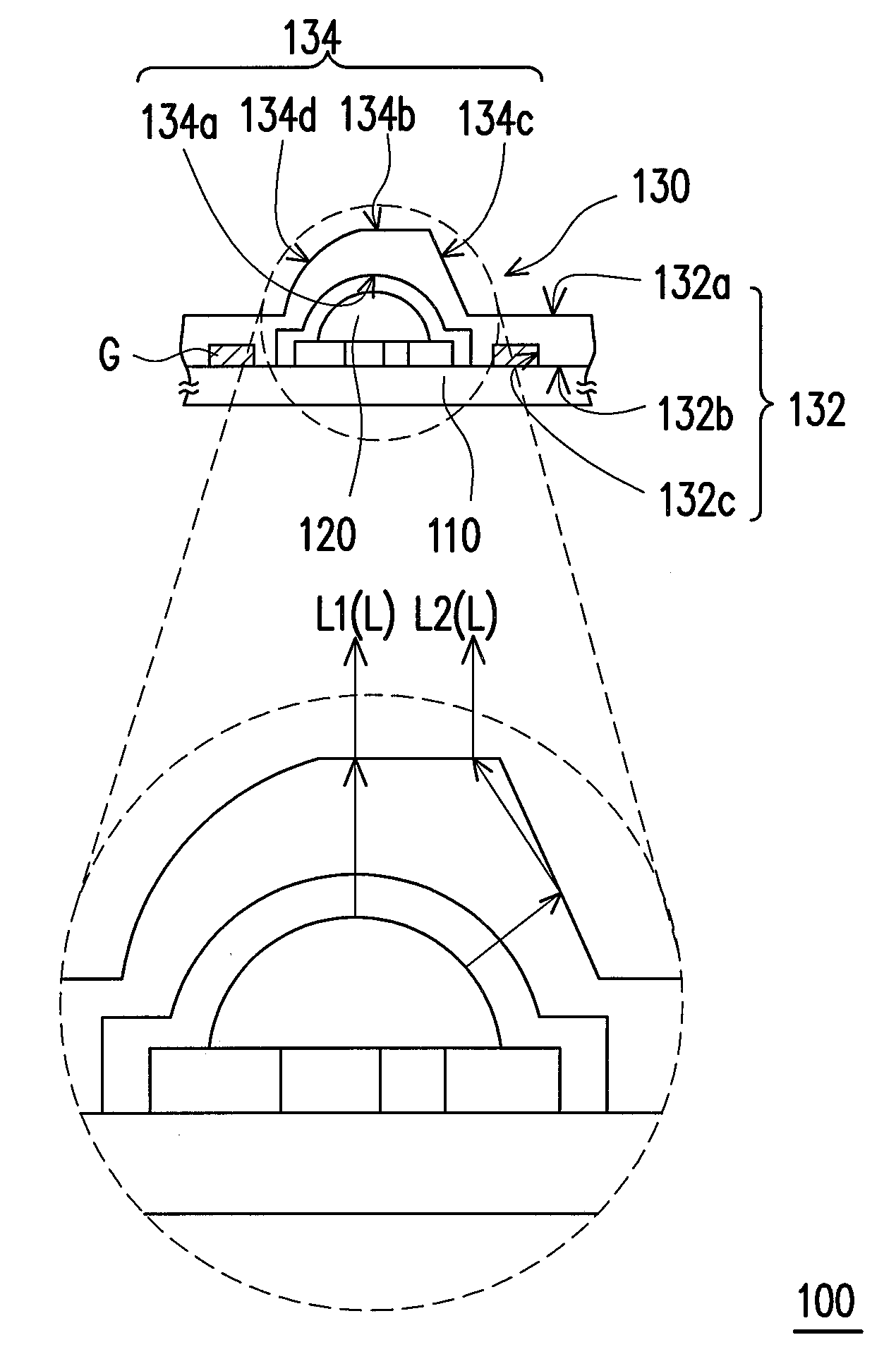
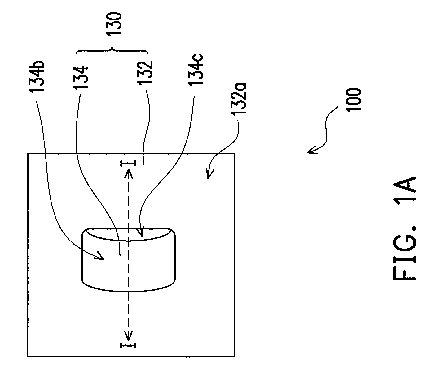
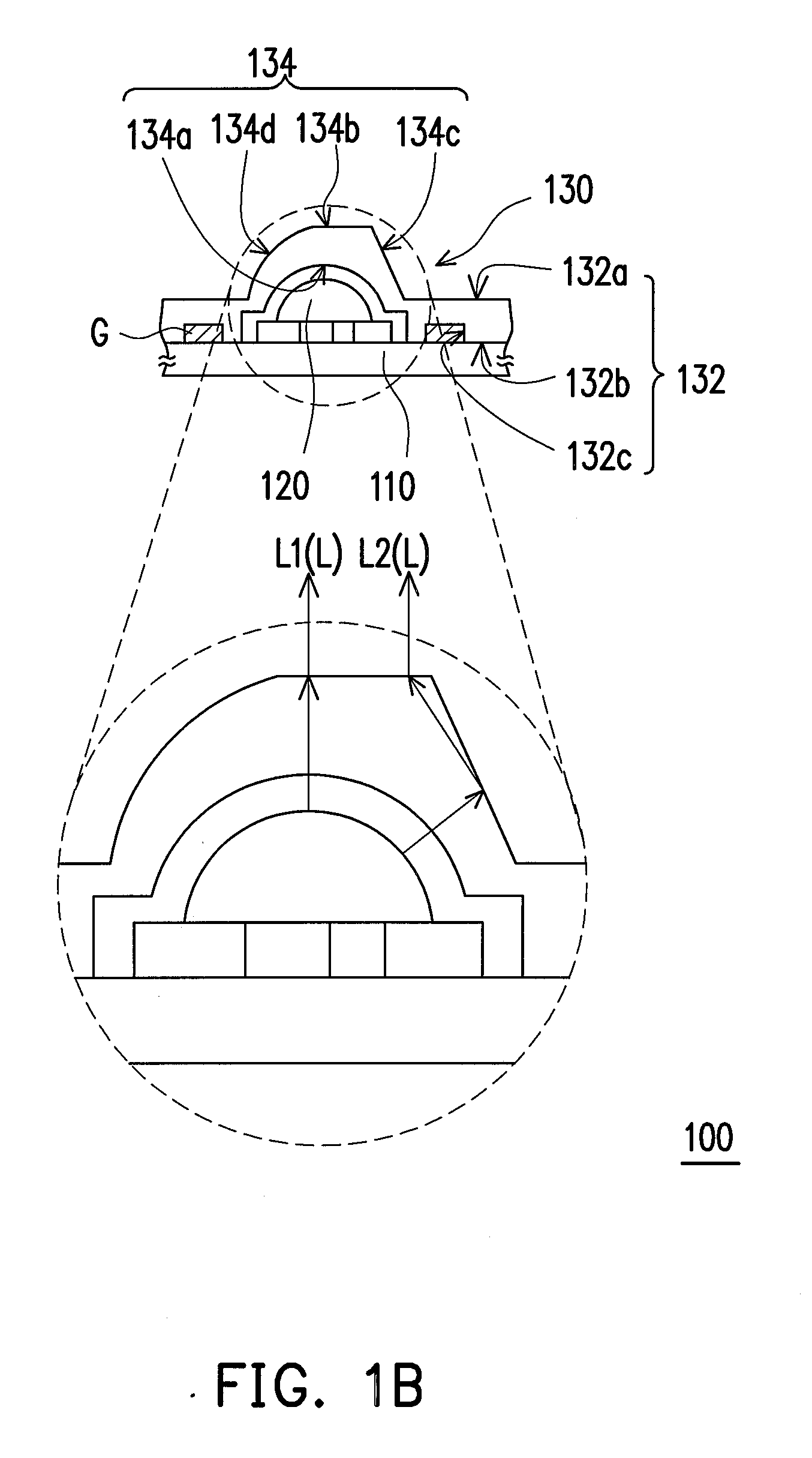
[0066]FIG. 1A is a schematic top view of a light emitting device according to an embodiment of the invention. FIG. 1B is a schematic side view taken along line I-I in FIG. 1A. FIG. 1C is a schematic back-side view of the transparent plate depicted in FIG. 1A. Referring to FIG. 1A, FIG. 1B, and FIG. 1C simultaneously, in the present embodiment, a light emitting device 100 includes a carrier 110, a light emitting element 120, and a transparent plate 130.

[0067]In details, the light emitting element 120 is disposed and electrically connected to the carrier 110. In the present embodiment, the light emitting element 120 is a light emitting diode (LED), and more specifically, this LED is a surface mount dev...


PUM


Abstract

A light emitting device includes a carrier, a light emitting element electrically connected to the carrier, a transparent plate having at least one through hole formed therein and including a flat-portion and a lens-portion and a permeable membrane structure disposed on a surface of the transparent plate. The lens-portion covers the light emitting element and has a light incident surface, a light emitting surface, a first and a second side surfaces. A first partial beam of the light beam passes through the light incident surface and leaves from the light emitting surface. A second partial beam of the light beam passes through the light incident surface and is transmitted to the first or the second side surface. The first or the second side surface reflects at least a part of the second partial beam of the light beam to be passed through the light emitting surface.

Description

CROSS-REFERENCE TO RELATED APPLICATION[0001]This application is a continuation in part application of and claims the priority benefit of U.S. application Ser. No. 12 / 703,201, filed on Feb. 10, 2010, now pending, which claims the priority benefit of Taiwan application Ser. No. 98137149, filed on Nov. 2, 2009. The prior U.S. application Ser. No. 12 / 703,201 is a continuation in part application of and claims the priority benefit of an U.S. application Ser. No. 12 / 610,371, filed on Nov. 2, 2009, now pending, which claims the priority benefit of Taiwan application no. 98105180, filed on Feb. 18, 2009. The entirety of each of the above-mentioned patent applications is hereby incorporated by reference herein and made a part of this specification.BACKGROUND OF THE INVENTION[0002]1. Field of the Invention[0003]The present invention relates to a light emitting device, more particularly, to a light emitting device with a better light emitting uniformity and efficiency.[0004]2. Description of R...

Claims


Application Information

Patent Timeline
Patent Type & Authority Applications(United States)
IPC IPC(8): H01L33/58H01L33/48H01L33/62
CPCF21K9/00F21V5/007F21V5/04F21V7/0083G02B19/0061F21Y2101/02F21Y2105/001G02B19/0028F21V31/04F21V31/03F21K9/69F21Y2105/10F21Y2115/10
Inventor TSAI, HSIN-CHANGLIANG, CHIA-HAOCHIANG, JEN-TA
Owner EVERLIGHT ELECTRONICS
Why Eureka
Try Eureka