Light emission device and display device including same

a technology of light emitting device and display device, which is applied in the manufacture of electrode systems, electric discharge tubes/lamps, and discharge tubes luminescnet screens, etc., can solve the problems of inability to bond with the sealing member portion, the manufacturing method is relatively complicated, and the manufacturing cost is relatively high. achieve the effect of suppressing vacuum leakage, improving terminal structure and simplifying manufacturing process

Inactive Publication Date: 2010-11-25
SAMSUNG SDI CO LTD
View PDF2 Cites 0 Cited by
  • Summary
  • Abstract
  • Description
  • Claims
  • Application Information

AI Technical Summary

Benefits of technology

[0009]Aspects of embodiments of the present invention are directed toward a light emitting device capable of simplifying its manufacturing process and / or suppressing vacuum leakage by improving its terminal structure, and a display device having the same.

Problems solved by technology

However, in such a connection structure, because a separate thick film and / or thin film process and bonding process should be performed, its manufacturing method is relatively complicated and its manufacturing cost is relatively high.
However, because the electron emission region and driving electrodes are formed on the rear substrate and a phosphor layer and an anode are formed on the front substrate, a bonding surface thereof that is formed may not be flat, and a portion in which bonding is formed with the sealing member may be inappropriate.
In this case, because vacuum of the vacuum chamber may leak, the vacuum degree may be deteriorated.

Method used


Image

  • Light emission device and display device including same
  • Light emission device and display device including same
  • Light emission device and display device including same

Examples


Embodiment Construction

[0033]The present invention will be described more fully hereinafter with reference to the accompanying drawings, in which exemplary embodiments of the invention are shown. As those skilled in the art would realize, the described embodiments may be modified in various different ways, all without departing from the spirit or scope of the present invention.

[0034]When it is stated that a first part, such as a layer, film, region, or plate, is positioned on a second part, it refers to that the first part is directly on the second part or on the second part with one or more intermediate parts therebetween. If a first part is stated to be positioned directly on a second part, it refers to that there is no intermediate part between the first and second parts.

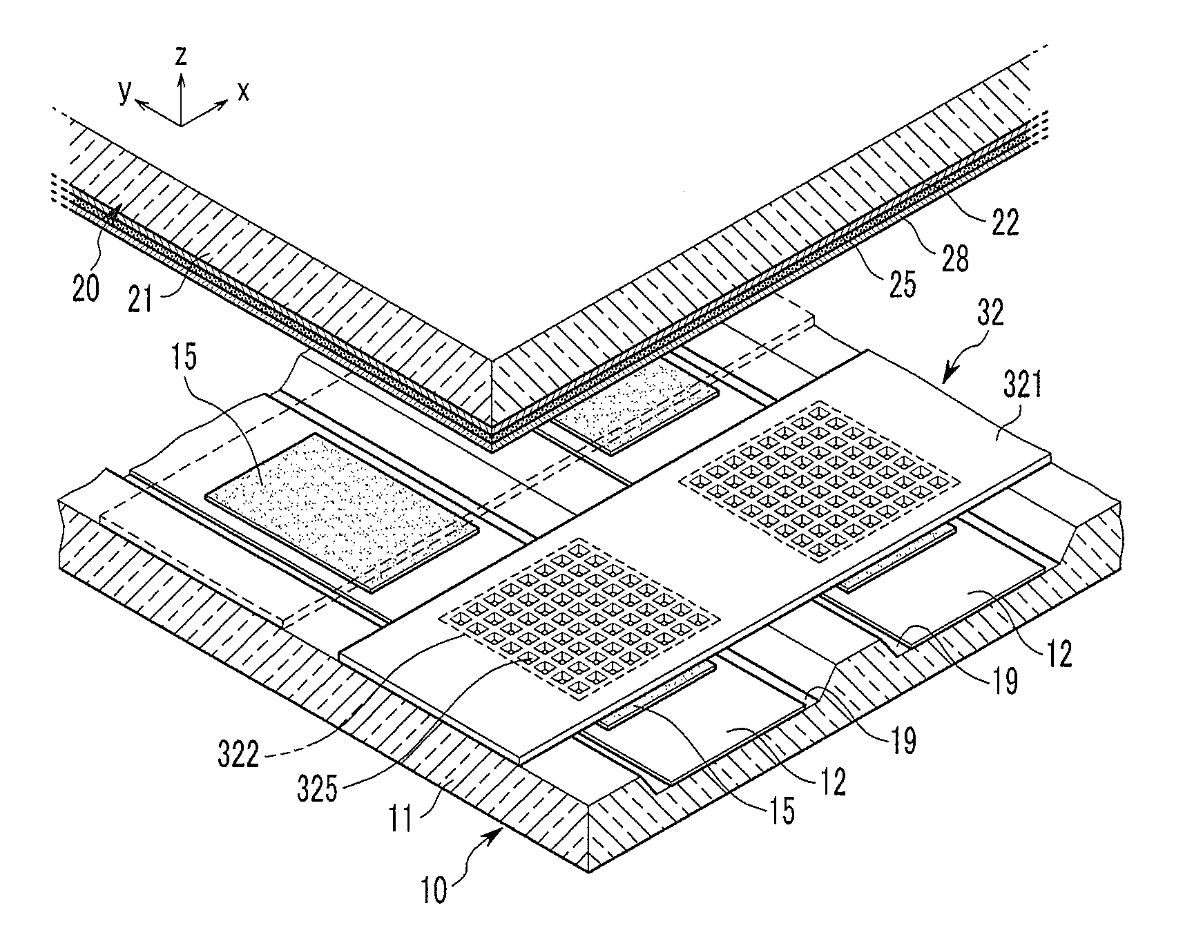
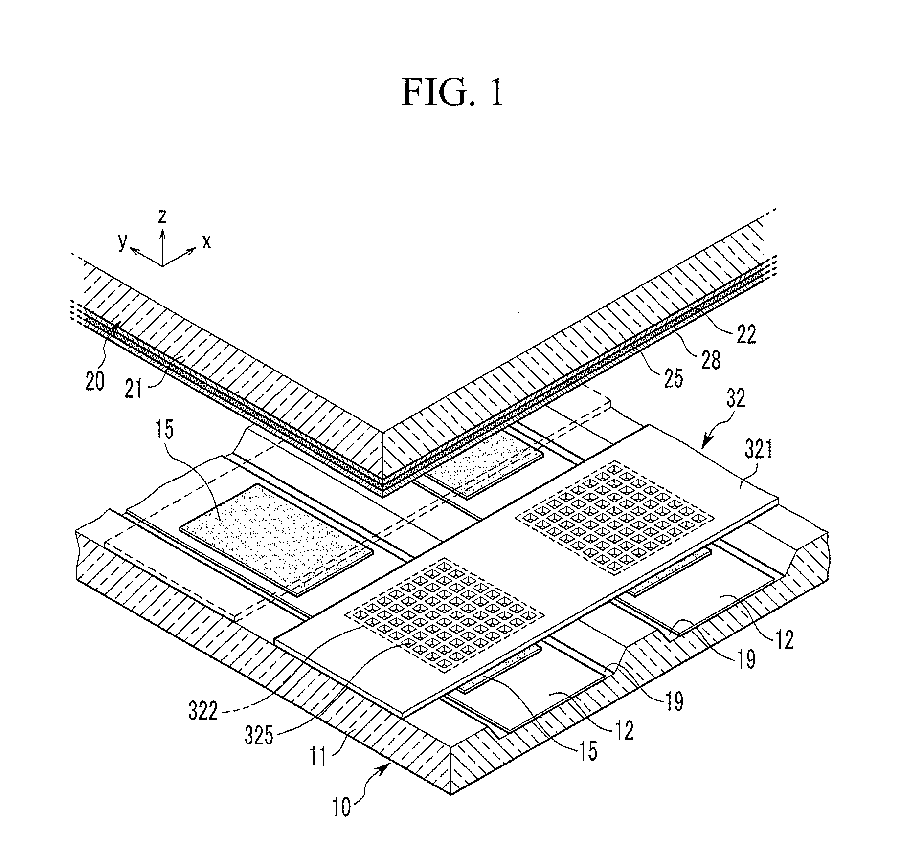
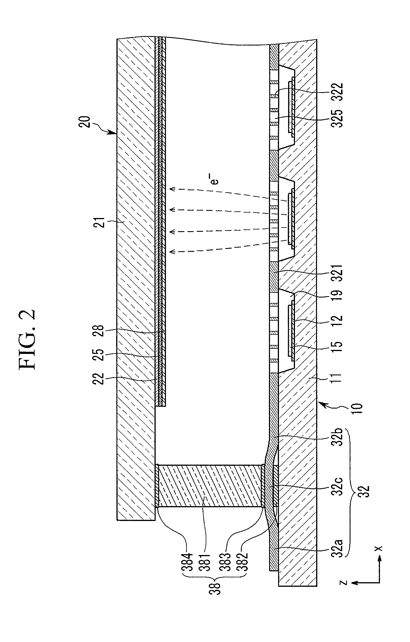
[0035]A light emitting device according to a first exemplary embodiment of the present invention will be described in more detail with reference to FIGS. 1 to 4.

[0036]FIG. 1 is a partial perspective view of a light emitting device acco...


PUM


Abstract

A light emitting device capable of simplifying its manufacturing process and/or suppress vacuum leakage by improving its terminal structure and a display device having the same. The light emitting device includes a first substrate assembly, a second substrate assembly, and a sealing member for bonding the first substrate assembly with the second substrate assembly. The first substrate assembly includes a first substrate main body having recess portions, first electrodes within the recess portions, electron emission regions on the first electrodes, and second electrodes at a distance away from the electron emission regions and fixed to a surface of the first substrate assembly. Here, a first portion of the second electrode including a first end portion of the second electrode is exposed out of a region surrounded by the seal member and out of the seal member and is used as a terminal connected to an external circuit.

Description

CROSS-REFERENCE TO RELATED APPLICATION[0001]This application claims priority to and the benefit of Korean Patent Application No. 10-2009-0045554, filed in the Korean Intellectual Property Office on May 25, 2009, the entire content of which is incorporated herein by reference.BACKGROUND[0002]1. Field[0003]The following description relates to a light emitting device and a display device having the same.[0004]2. Description of Related Art[0005]A light emitting device can emit light and include a front substrate having a phosphor layer and an anode thereon and a rear substrate having an electron emission region and driving electrodes thereon. The front substrate and the rear substrate form a vacuum chamber together with a sealing member by integrally bonding edges (or edge portions) thereof by the sealing member and exhausting the internal space. In the light emitting device, electrons that are emitted toward the front substrate from the electron emission region excite the phosphor laye...

Claims


Application Information

Patent Timeline
Patent Type & Authority Applications(United States)
IPC IPC(8): H01J1/62
CPCH01J9/268H01J63/02H01J61/305H01J1/30
Inventor SEON, HYEONG-RAELEE, JAE-YOUNGCHANG, DONG-SU
Owner SAMSUNG SDI CO LTD
Why Eureka
Try Eureka