Display device and active matrix substrate

Inactive Publication Date: 2010-11-25
SHARP KK
View PDF15 Cites 10 Cited by
  • Summary
  • Abstract
  • Description
  • Claims
  • Application Information

AI Technical Summary

Benefits of technology

[0007]Photodiodes used as light sensors in a display device, are subject to noise (electric noise) caused by variation in electric potentials in pixel electrodes within pixels. Th

Problems solved by technology

Photodiodes used as light sensors in a display device, are subject to noise (electric noise) caused by variation in electric potentials in pixel electrodes within

Method used


Image

  • Display device and active matrix substrate
  • Display device and active matrix substrate
  • Display device and active matrix substrate

Examples


Embodiment Construction

[0048]The following describes an embodiment of the present invention. Note that, the present embodiment describes an example in which a display device of the present invention is applied to a light sensor touch panel built-in liquid crystal display device.

[0049]The following describes a gross structure of a liquid crystal display device of the present embodiment in reference to FIG. 1 and FIG. 2.

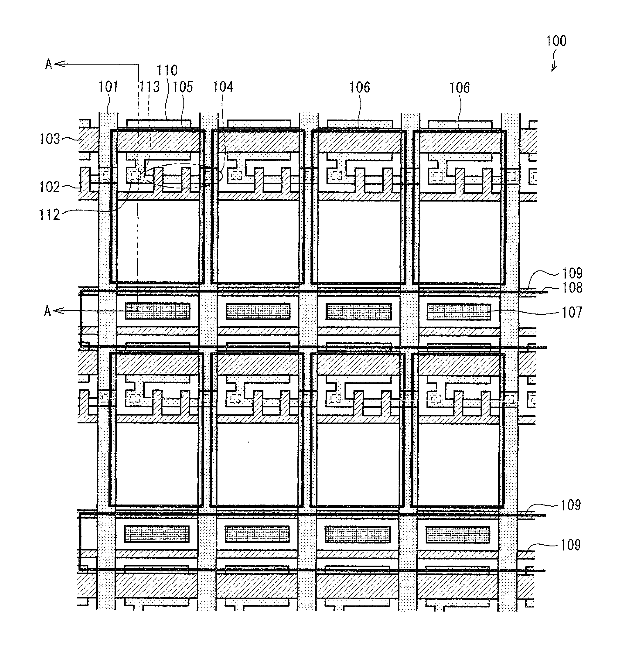
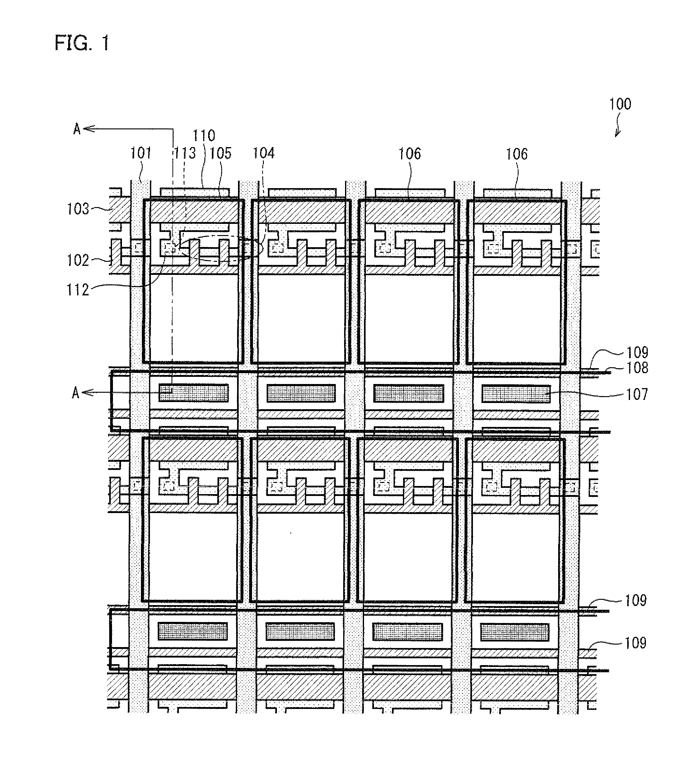
[0050]FIG. 1 is a plain view of a liquid crystal display device of the present embodiment. Note that, in FIG. 1, for convenience in description, only a side of an active matrix substrate (hereinafter referred to as a TFT (Thin Film Transistor) array substrate) is described, and a liquid crystal and a counter substrate are not shown.

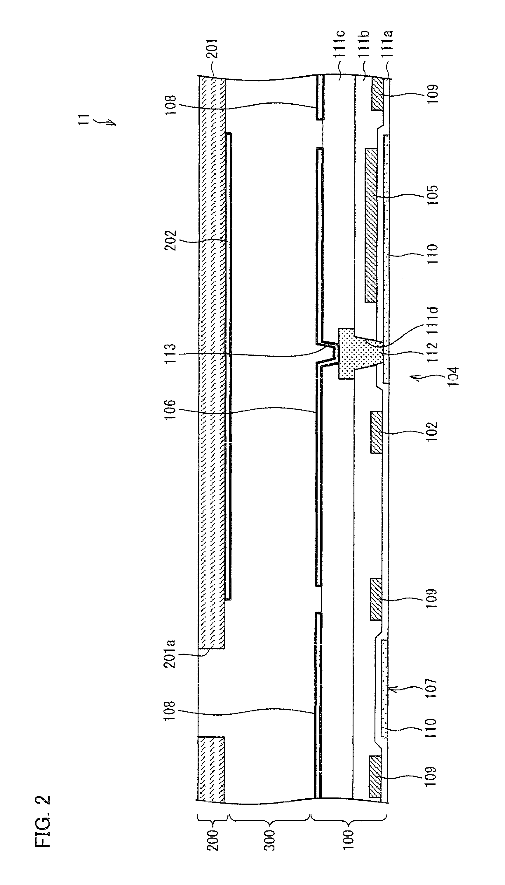
[0051]FIG. 2 is a cross-sectional view taken along line A-A of the liquid crystal display device shown in FIG. 1. Note that FIG. 2 shows not only the TFT array substrate but also the liquid crystal and the counter substrate. That is to say, as shown in FIG. 2, a l...


PUM


Abstract

A liquid crystal display device of the present invention includes a liquid crystal layer between a TFT array substrate and a counter substrate. The TFT array substrate has photo sensor elements in pixels, and has transparent shield electrodes which cover the photo sensor elements provided. The transparent shield electrodes are electrically insulated from pixel electrodes. Therefore, in the liquid crystal display device, an effect of electric noise on the photo sensor elements can be reduced for avoiding deterioration of sensitivity of the photo sensor elements.

Description

TECHNICAL FIELD[0001]The present invention relates to a display device including a display panel in which a light sensor is provided in each pixel.BACKGROUND ART[0002]Conventionally, a display device including a display panel in which a light sensor is provided in each pixel has been proposed.[0003]In the display device, a photodiode is generally used as the light sensor. A sensitivity of the photodiode is generally indicated by S (signal) / N (noise) ratio. That is, if the S / N ratio is large, it means the photodiode is sensitive.[0004]For improvement in the sensitivity of the light sensor in the display panel having the light sensor in each pixel, Patent Literature 1, for example, discloses a technique in which two photodiodes are provided in one pixel to increase a photocurrent thereby to improve the S (signal) / N (noise) ratio. That is, in the technique disclosed in Patent Literature 1, the photocurrent that contributes to S (signal) of the S / N ratio indicating the sensitivity of th...

Claims


Application Information

Patent Timeline
IPC IPC(8): G09G3/20
CPCG02F1/13318G02F1/133555G02F1/1343G06F3/042G02F2001/13312G02F2001/136218G06F3/0412G02F1/136286G02F1/13312G02F1/136218
Inventor YOSHIDA, KEISUKEMAEDA, KAZUSHIROYAYOTANI, RYOHJIFUJIWARA, MASARIRO
Owner SHARP KK
Why Eureka
Try Eureka