Gas sensor

a technology of gas sensor and sensor body, which is applied in the field of gas sensor, can solve the problems achieve the effects of deterioration of sensitivity of gas sensor, excellent detection accuracy, and inexpensive manufacturing

Active Publication Date: 2006-08-24
NGK SPARK PLUG CO LTD
View PDF9 Cites 6 Cited by
  • Summary
  • Abstract
  • Description
  • Claims
  • Application Information

AI Technical Summary

Benefits of technology

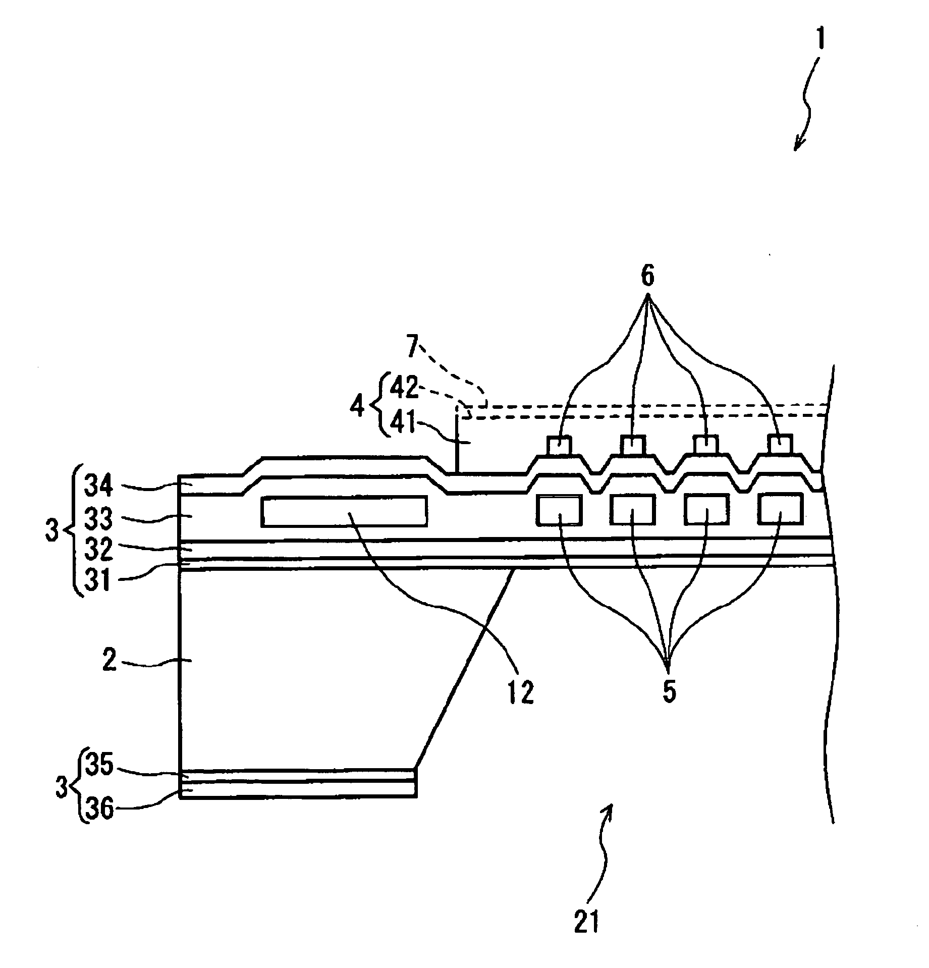
[0012] In a first aspect of the present invention, a catalytic portion (catalyst substance) is dispersedly formed on a surface of a metal-oxide semiconductor portion, and an insulating portion is dispersedly formed on the surface of the metal-oxide semiconductor portion where the catalytic portion is formed (i.e. on a gas sensing portion). The first surface additive rate, which is expressed by Si / (M+Si), of the metal-oxide semiconductor portion is determined to be 65% or more to 97% or less, and the second surface additive rate, which is expressed by Si / (Sn+Si), of the same is determined to be 75% or more to 97% or less. That is, the metal-oxide semiconductor portion and the catalytic portion which constitute the gas sensing portion are exposed to the surface of the insulating portion so that the negative charge of the oxygen (O2−) in the atmosphere may be adsorbed on to the surface of the metal-oxide semiconductor portion, thereby functioning as a gas sensor. Furthermore, SiO2 constituting the insulating portion has a characteristic which traps hydroxyl group OH−, preventing OH− from being adsorbed on to an O2−adsorption site of the metal-oxide semiconductor portion in a high temperature and high humidity atmosphere. The gas sensor of the present invention may demonstrate excellent detection accuracy and humidity resistance because the catalytic portion and the insulating portion are formed on the surface of the metal-oxide semiconductor portion so that the surface additive rate thereof may be within the above-mentioned ranges.
[0013] When the first surface additive rate expressed by Si / (M+Si) of the metal-oxide semiconductor portion is less than 65%, or when the second surface additive rate expressed by Si / (Sn+Si) of the same is less than 75%, a proportion where the metal-oxide semiconductor portion and the catalytic portion are exposed in between the insulating portions will be large. As a result, the proportion of the insulating portion will be relatively small, causing hydroxyl group OH31 to be unlikely to be trapped in a high temperature and high humidity atmosphere whereby the sensitivity of the gas sensor (proportion of resistance value in the metal-oxide semiconductor portion when a gas to be detected is present vs. absent) will deteriorate. On the other hand, when the first surface additive rate expressed by Si / (M+Si) of the metal-oxide semiconductor portion is larger than 97%, or when the second surface additive rate expressed by Si / (Sn+Si) of the same is larger than 97%, a proportion where the metal-oxide semiconductor portion and the catalytic portion are exposed in between the insulating portions will be small. That is, since the O2− adsorption site of the gas sensor lessens, irrespective of the existence of the gas to be detected, the resistance of the metal-oxide semiconductor portion will hardly change (i.e. remain at a large value), resulting in a deterioration of the sensitivity of the gas sensor.
[0014] Moreover, since the insulating portion is comprised mainly of SiO2, it may be inexpensively manufactured, as well as reducing environmental load.
[0015] In addition, in the present invention, the surface additive rate is obtained from the number of atoms measured by an X-ray photoelectron spectroscopy (XPS). In detail, a photoelectron peak area of an element subjected to a measurement among the elements existing on the metal-oxide semiconductor portion is measured by an X-ray surface analyzer (e.g., Quantera SXM, manufactured by Physical Electronics) on the condition that a detection depth is 4-5 nm (45 degrees of extraction angles) in the detection area of 100 μm, using an A1K α ray (1486 keV). Then, the number of atoms of each element, which is subjected to the measurement, is determined quantitatively (relative determinate quantity) by the equation shown in (1). The above-mentioned surface additive rate is calculated according to the number of atoms of thus-determined quantity of each element.
[0016] wherein, Ci shall represent a determined quantity value (atomic%) of the element i subjected to the measurement, Ai shall represent a photoelectron peak area of the element i subjected to the measurement, and RSFi shall represent a relative sensitivity coefficient of the element i subjected to the measurement.
[0017] Moreover, in the present invention, “Main component” denotes a component that occupies 80% by weight or more, preferably 90% by weight or more, further preferably 95% by weight or more of the total components contained.

Problems solved by technology

Since the metal-oxide semiconductor is susceptible to humidity, the sensitivity of the gas sensor tends to deteriorate under the influence of humidity.
Thus, when the humidity in the measurement atmosphere increases, the sensitivity of the gas sensor deteriorates.

Method used


Image

  • Gas sensor
  • Gas sensor
  • Gas sensor

Examples


first embodiment

[0035] In order to confirm the effect of the present invention regarding the gas sensor 1 described above, seven samples each having different surface additive rate (of Si in the metal-oxide semiconductor portion 41, a noble metal M constituting the catalytic portion 42 and Sn) were produced based on each process explained below, and then they were subjected to an evaluation. In addition, an unfinished article of the gas sensor 1 in the production process will be called a substrate.

[0036] (1) Rinsing of Silicon Substrate 2[0037] First, a silicon substrate 2 having a thickness of 400 μm was immersed in a rinsing liquid and subjected to a rinsing treatment.

[0038] (2) Formation of Insulating Layers 31, 35[0039] The silicon substrate 2 was put into a heat treatment furnace and subjected to a thermal-oxidization treatment to form a silicon oxide layer (insulating layers 31 and 35) having a thickness of 100 nm all over the silicon substrate 2.

[0040] (3) Formation of Insulating Layers 3...


PUM

PropertyMeasurementUnit
humidityaaaaaaaaaa
temperatureaaaaaaaaaa
thicknessaaaaaaaaaa

Abstract

The present invention provides a gas sensor having excellent humidity resistance even if used in a high temperature and high humidity atmosphere. According to the present invention, a gas sensor is comprised of: a silicon substrate; a metal-oxide semiconductor portion comprised mainly of SnO2 and formed on the substrate; and a catalytic portion comprised of Pd and dispersed on a surface of the metal-oxide semiconductor portion, wherein the metal-oxide semiconductor portion and the catalytic portion constitute a gas sensing portion. Furthermore, an insulating portion comprised mainly of SiO2 is formed dispersedly on a surface of the gas sensing portion. Further, the catalytic portion and the insulating portion are formed on the surface of the metal-oxide semiconductor portion so that the surface additive rate, which is expressed by Si/(Pd+Si) representing the ratio in the number of atoms of Si to Pd, of the gas sensing portion having the insulating portion may be 65% or more to 97% or less, and so that the surface additive rate, which is expressed by Si/(Sn+Si) representing the ratio in the number of atoms of Si to Sn, of the gas sensing portion may be 75% or more to 97% or less.

Description

FIELD OF INVENTION [0001] The present invention relates to a gas sensor employing a metal-oxide semiconductor. BACKGROUND OF THE INVENTION [0002] Conventionally, it is known that a gas sensor employs a metal-oxide semiconductor, such as tin oxide (SnO2) as a sensitive layer, and is capable of (a) detecting whether or not a gas to be detected is present, or (b) detecting a concentration variance thereof by means of a change in electrical characteristics (e.g., change in resistance) of the metal-oxide semiconductor. The metal-oxide semiconductor used in the gas sensor has a characteristic in which the number of conduction electrons in the metal-oxide semiconductor decreases and the resistance increases due to adsorption of the negative charge of oxygen (O2−) in the atmosphere on to the surface of the metal-oxide semiconductor. In such a state, if any reducing gas (such as carbon monoxide) is present as a gas to be detected in a measurement atmosphere, O2−adsorbed on to the surface of ...

Claims


Application Information

Patent Timeline
Patent Type & Authority Applications(United States)
IPC IPC(8): G01N7/00
CPCG01N27/125A61B17/50A61B2017/320004
Inventor NAKAGAWA, SHINICHINAKANO, YOSHIHIROKIDA, MASAHITOKOJIMA, TAKIO
Owner NGK SPARK PLUG CO LTD
Why Eureka
Try Eureka