Solid state image sensor, method of manufacturing solid state image sensor, and image capturing system

a solid-state image sensor and manufacturing method technology, applied in the direction of electrical equipment, semiconductor devices, radio frequency control devices, etc., can solve the problems of receiving units, deterioration in sensitivity and image quality of solid-state image sensors, and inability to contribute to the focusing of light, so as to reduce the deterioration in sensitivity and image quality

Active Publication Date: 2016-08-11
CANON KK
View PDF2 Cites 5 Cited by
  • Summary
  • Abstract
  • Description
  • Claims
  • Application Information

AI Technical Summary

Benefits of technology

[0006]The present invention provides a solid state image sensor advantageous in reducing deterioration in sensitivity and image quality.

Problems solved by technology

In principle, however, each microlens having the teardrop shape disclosed in Japanese Patent Laid-Open No. 2007-335723 cannot cause part of light entering the microlens to enter the corresponding light-receiving unit, that is, cannot contribute to the focusing of light, depending on the incident position of light.
In addition, such light is likely to enter the regions of adjacent pixels and become stray light, leading to deterioration in the sensitivity and image quality of the solid state image sensor.

Method used


Image

  • Solid state image sensor, method of manufacturing solid state image sensor, and image capturing system
  • Solid state image sensor, method of manufacturing solid state image sensor, and image capturing system
  • Solid state image sensor, method of manufacturing solid state image sensor, and image capturing system

Examples


first embodiment

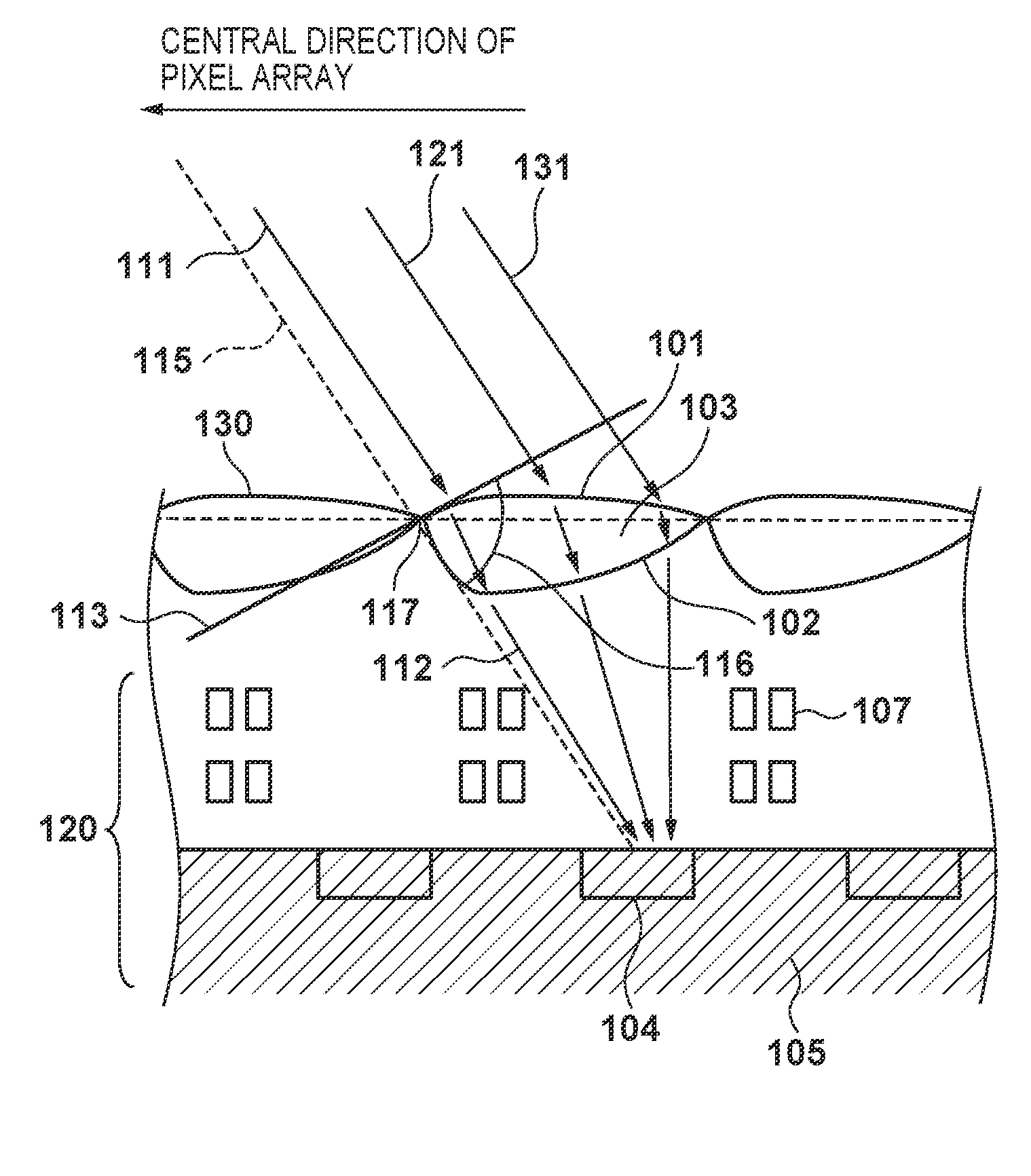
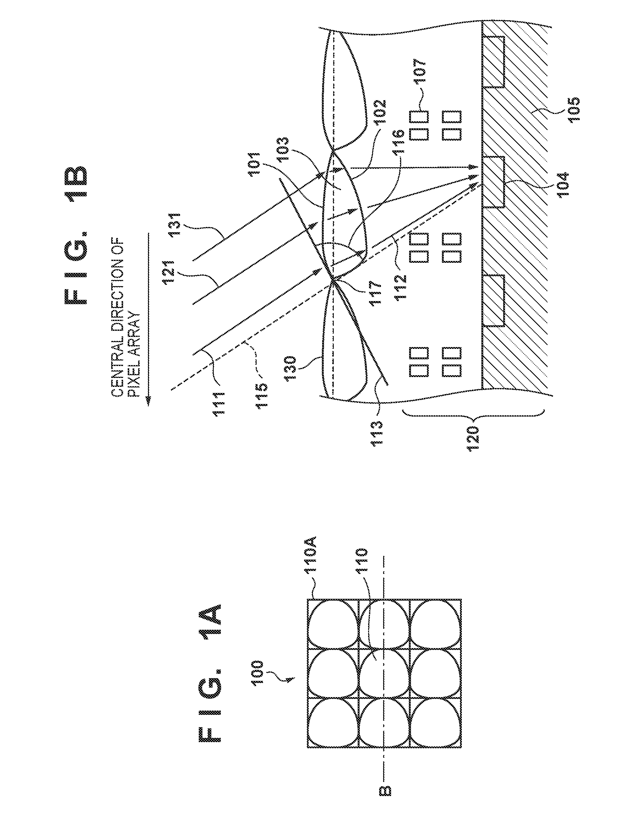
[0018]FIGS. 1A and 1B are schematic views showing the arrangement of a solid state image sensor 100 according to one aspect of the present invention. FIG. 1A is a plan view of the solid state image sensor 100. FIG. 1B is a sectional view taken along a chain line B of the solid state image sensor 100 shown in FIG. 1A. As shown in FIG. 1A, the solid state image sensor 100 includes a pixel array 110A in which a plurality of pixels 110 are arranged.

[0019]As shown in FIG. 1B, a solid state image sensor substrate 120 forming the solid state image sensor 100 includes a semiconductor substrate 105, photoelectric conversion devices (light-receiving units) 104 formed in the semiconductor substrate 105, and a wiring layer 107 in which transistors (not shown) and wirings are formed. The solid state image sensor 100 implements a function of reading out light (incident light) entering each photoelectric conversion device 104 as an electrical signal upon photoelectric conversion. Microlenses 103 w...

second embodiment

[0036]A method of manufacturing a solid state image sensor 100 according to one aspect of the present invention will be described with reference to FIGS. 7A to 7E. First of all, photoelectric conversion devices 104, transistors (not shown), a wiring layer 107, and the like are formed in and on a semiconductor substrate 105 by using techniques known in the art, thereby preparing a solid state image sensor substrate 120.

[0037]As shown in FIG. 7A, the surface of the solid state image sensor substrate 120 is coated with a photoresist (photoresist film) 701 for the formation of a second lens material having a lower refractive index than a first lens material formed in a subsequent process.

[0038]Subsequently, the photoresist 701 applied on the surface of the solid state image sensor substrate 120 is exposed and developed by using a mask exhibiting a continuous tone change. Such a mask is a mask for the formation of microlenses 103. For example, this mask includes a gray mask or an area to...


PUM


Abstract

The present invention provides a solid state image sensor including a pixel array having a plurality of pixels arranged therein, each of the plurality of pixels including a photoelectric conversion device and a microlens configured to guide incident light to the photoelectric conversion device, the microlens having a lower surface, on an exit side of the incident light, which has a convex shape with respect to the photoelectric conversion device, with a vertex of the convex shape shifting from a center position of the microlens to a central side of the pixel array.

Description

BACKGROUND OF THE INVENTION[0001]1. Field of the Invention[0002]The present invention relates to a solid state image sensor, a method of manufacturing a solid state image sensor, and an image capturing system.[0003]2. Description of the Related Art[0004]Solid state image sensors and display apparatuses use optical elements such as microlens arrays as disclosed in Japanese Patent Laid-Open No. 2007-335723. Japanese Patent Laid-Open No. 2007-335723 discloses a technique of providing microlenses, each having a shape called a teardrop, in a solid state image sensor to efficiently focus light entering from oblique directions onto light-receiving units. Such a microlens is shaped to have a curved shape tapering to the outside of the solid state image sensor and having a vertex at an outside end portion when viewed in a planar view.[0005]In principle, however, each microlens having the teardrop shape disclosed in Japanese Patent Laid-Open No. 2007-335723 cannot cause part of light entering...

Claims


Application Information

Patent Timeline
Patent Type & Authority Applications(United States)
IPC IPC(8): H01L27/146
CPCH01L27/14627H01L27/14685H01L27/14636H01L27/14621H01L27/14605
Inventor SEKINE, YASUHIRO
Owner CANON KK
Why Eureka
Try Eureka