Image sensor and image-capturing device

Pending Publication Date: 2018-10-11
NIKON CORP
View PDF9 Cites 4 Cited by
  • Summary
  • Abstract
  • Description
  • Claims
  • Application Information

AI Technical Summary

Benefits of technology

The patent text explains that when there is a need for high-speed readouts (up to 10000 frames / sec), the exposure time reduces. This means that the amount of electric charge generated by photoelectric conversion decreases, which leads to a decrease in sensitivity. The technical effect of this is that it affects the ability of the device to capture and convert light into an electric signal with high accuracy and speed.

Problems solved by technology

However, in high speed readout (e.g., 100 to 10000 frames / sec) required in recent years, exposure time reduces.
Therefore, the amount of electric charge generated by photoelectric conversion decreases, which lead to a deterioration in the sensitivity.

Method used


Image

  • Image sensor and image-capturing device
  • Image sensor and image-capturing device
  • Image sensor and image-capturing device

Examples


first embodiment

[0030]Schematic Element Structure

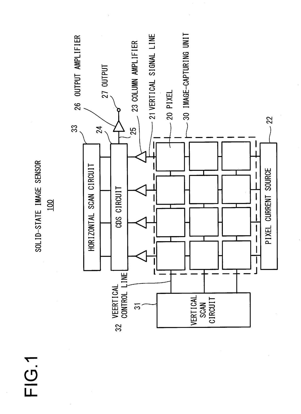
[0031]FIG. 1 is a view illustrating a schematic configuration of a solid-state image sensor 100 according to a first embodiment.

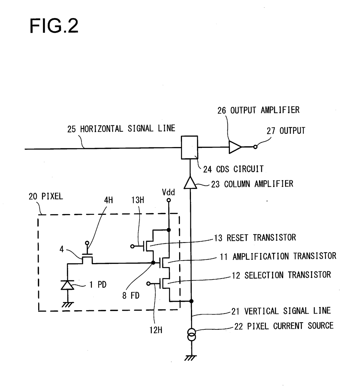
[0032]The solid-state image sensor 100 includes an image-capturing unit 30 having pixels 20 arranged on a light receiving surface. The pixels 20 are supplied with drive pulses from a vertical scan circuit 31 via vertical control lines 32. Further, the pixels 20 are connected to vertical signal lines 21 on a column basis. The vertical signal lines 21 are connected to a pixel current source 22.

[0033]Furthermore, noise outputs and signal outputs that are time-divisionally outputted from the pixels 20 to the vertical signal lines 21 are sequentially inputted to a CDS circuit (a correlated double sampling circuit) 24 via column amplifiers 23. The CDS circuit 24 calculates a difference between both outputs to generate a true signal output. This true signal output is horizontally scanned by a drive signal from a horizontal scan cir...

second embodiment

Third Variation of Second Embodiment

[0148]FIG. 13 is a view illustrating a configuration of a solid-state image sensor 100D according to a third variation of the second embodiment, and it corresponds to FIG. 7 for the second embodiment. An equivalent circuit of the solid-state image sensor 100D in FIG. 13 is illustrated in FIG. 12. The same parts as those in FIGS. 7 and 4(b) are denoted by the same reference signs, and differences will be mainly described.

[0149]In the solid-state image sensor 100A in FIG. 6, the FD 8 is connected to the back gate electrode of the amplification transistor 11 without wiring, and the predetermined potential (e.g., the reference potential Vdd) is applied to the top gate electrode 11g. Contrastingly, in the solid-state image sensor 100D in FIG. 13, the top gate electrode of the amplification transistor 11 is connected to the FD 8 without wiring, and the back gate electrode of the amplification transistor 11 directly connects the GND terminal to the p reg...

fourth embodiment

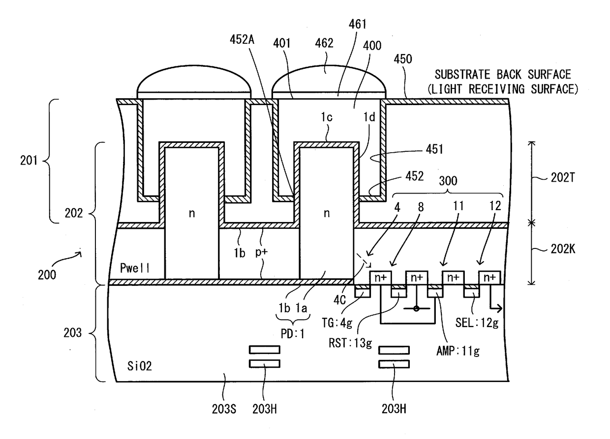
[0158]FIG. 15 is a view illustrating a configuration of a solid-state image sensor 100F according to a fourth embodiment, and it corresponds to FIG. 14 for the third embodiment. The same parts as those in FIG. 14 are denoted by the same reference signs, and differences will be mainly described.

[0159]The solid-state image sensor 100E according to the third embodiment is a so-called back illumination type element. The solid-state image sensor 100F according to the fourth embodiment is a front illumination type element in which a wiring region is arranged on the light receiving surface side. The wiring 203H is formed in a region further outside of the optical path region 400, that is, the oxide film 201 on the light receiving surface side. Other parts of the configuration are the same as those in the third embodiment and an explanation thereof will thus be omitted.

[0160]The solid-state image sensor 100F according to the fourth embodiment can also achieve similar advantageous effects as...


PUM


Abstract

An image sensor includes: a semiconductor substrate having a light receiving unit that receives incident light passed through a microlens; and a light shielding unit that blocks a part of the light passed through the microlens and enters the semiconductor substrate. The light receiving unit receives the incident light passed through the microlens, between the microlens and the light shielding unit.

Description

TECHNICAL FIELD[0001]The present invention relates to an image sensor and an image-capturing device.BACKGROUND ART[0002]PTL1 discloses the following solid-state image sensor.[0003]A semiconductor substrate is provided with an image-capturing region including a photoelectric conversion unit and a signal scan circuit unit and having unit pixels arranged in a matrix. The image-capturing region includes an field isolation insulating film that is provided to correspond to a boundary portion between adjacent unit pixels and surround each unit pixel; a MOSFET provided on a front surface of the semiconductor substrate and in a region below the field isolation insulating film; and a first diffusion layer having a first conductive type provided in a region in the vicinity of the field isolation insulating film in the semiconductor substrate. The field isolation insulating film is provided in the semiconductor substrate at an offset from the front surface of the semiconductor substrate on whic...

Claims


Application Information

Patent Timeline
IPC IPC(8): H01L27/146H04N5/378
CPCH01L27/14627H01L27/14623H01L27/14625H01L27/14609H01L27/14612H01L27/14643H04N5/378H01L27/14636H01L27/14629H01L27/1464H01L31/0232H01L27/14603H04N25/75
Inventor ISHIDA, TOMOHISAWATANABE, YOSHIYUKI
Owner NIKON CORP
Why Eureka
Try Eureka