Photoelectric conversion element and photoelectric conversion device

Active Publication Date: 2019-03-07
SONY CORP
View PDF0 Cites 3 Cited by
  • Summary
  • Abstract
  • Description
  • Claims
  • Application Information

AI Technical Summary

Benefits of technology

[0007]In the photoelectric conversion element and the photoelectric conversion device according to the respective embodiments of the disclosure, the isoelectronic trap region is provided in the region in which the depletion region is to be formed. Thus, electrons are trapped in the isoelectronic trap region, which provides rough determination of locations where the electrons are present. This causes expansion of k space by Heisenberg's uncertainty principle. As a result, direct-transition-like generation is carried out, leading to enhancement in photoelectric conversion efficiency.
[0008

Problems solved by technology

However, Si and Ge are semiconductors of an indirect transition type and have a concern that sensitivity drops sharply particularly in a near infrared region.
In this case, however, it is necessary to implant impurities

Method used


Image

  • Photoelectric conversion element and photoelectric conversion device
  • Photoelectric conversion element and photoelectric conversion device
  • Photoelectric conversion element and photoelectric conversion device

Examples


first embodiment

1. First Embodiment

[Configuration]

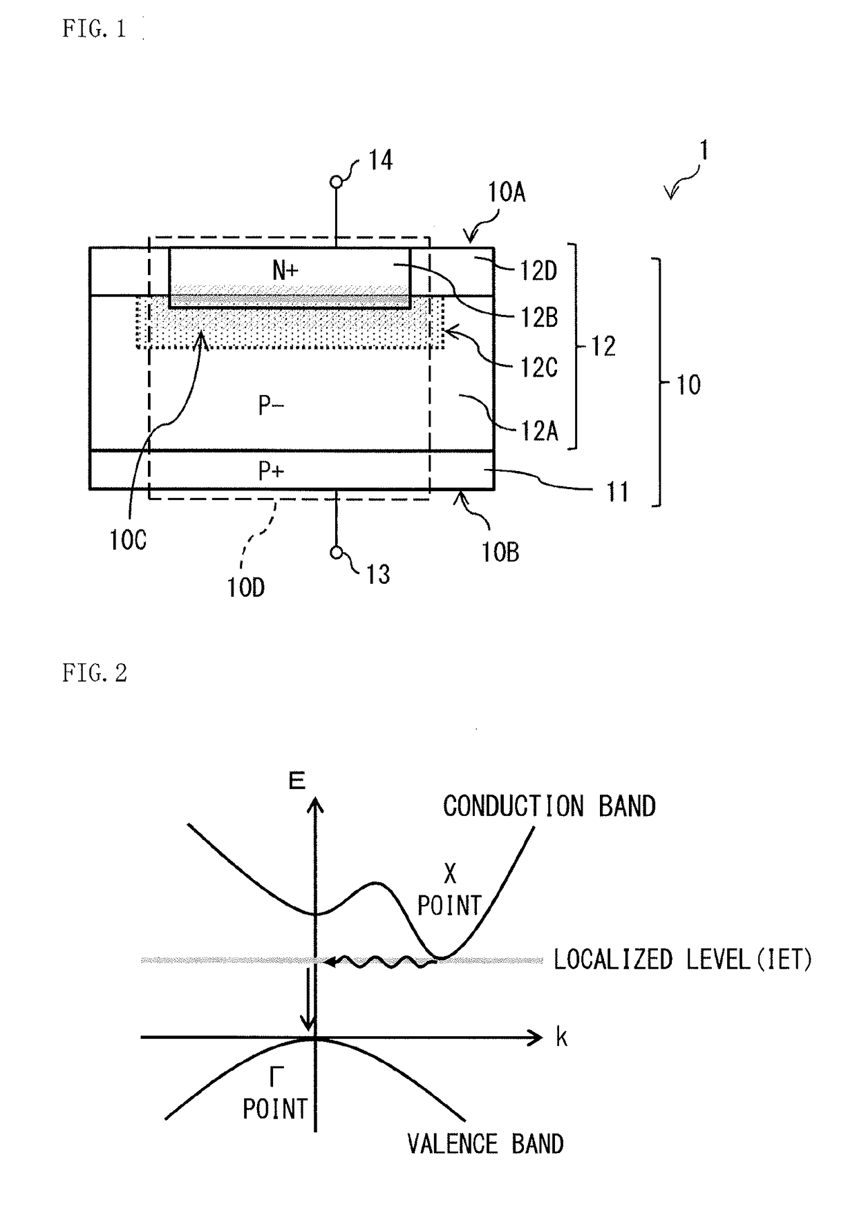
[0039]FIG. 1 illustrates an example of a cross-sectional configuration of a photoelectric conversion element I according to a first embodiment of the disclosure. The photoelectric conversion element 1 includes a photoelectric conversion region 10D inside a semiconductor layer 10. The photoelectric conversion region 10D includes a region in which a depletion region 10C is to be formed by voltage application to the semiconductor layer 10. The depletion region 10C is a region nearly devoid of electrons or holes as carriers. The depletion region 10C converts light into a photoelectron, in which the light enters from side on which a light receiving surface 10A (first main surface) is disposed. The photoelectric conversion region 10D generates the depletion region 10C by voltage application to the photoelectric conversion region 10D. Upon the light entering the depletion region 10C generated, the photoelectric conversion region 10D converts the photoelect...

second embodiment

[Configuration]

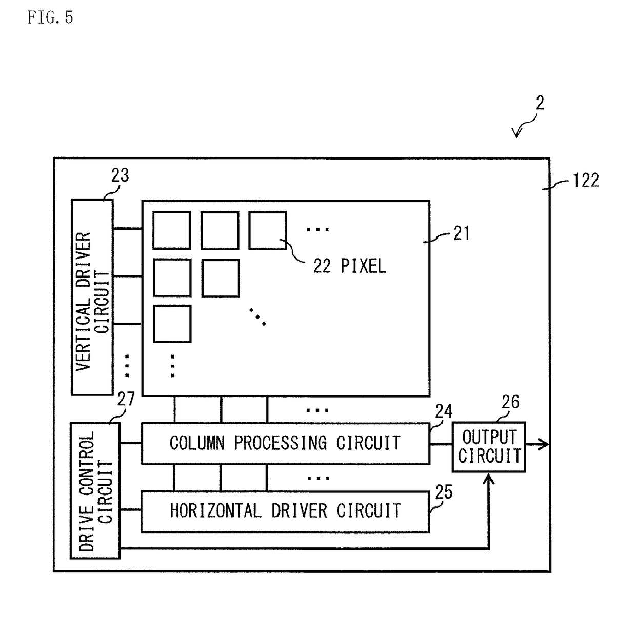
[0056]FIG. 5 illustrates an example of a schematic configuration of an imaging device 2 (photoelectric conversion device) according to a second embodiment of the disclosure. The imaging device 2 includes a plurality of photodiodes PD (photoelectric conversion elements) and a driver section that drives the one or more photodiodes PD (photoelectric conversion elements). The plurality of the photodiodes PD share a semiconductor layer 122 with one another, and are two-dimensionally disposed in a light receiving surface 122a (first main surface) of the semiconductor layer 122 shared by the plurality of the photodiodes PD.

[0057]The imaging device 2 includes a solid-state imaging element of a CMOS type. The imaging device 2 includes a pixel region 21 and a peripheral circuit. In the pixel region 21, a plurality of pixels 22 are disposed in rows and columns. The imaging device 2 includes, as the peripheral circuit, for example, a vertical driver circuit 23, a column processin...

third embodiment

3. Third Embodiment

[Configuration]

[0080]FIG. 15 illustrates an example of a cross-sectional configuration of a photoelectric conversion element 3 according to a third embodiment of the disclosure. The photoelectric conversion element 3 includes a photoelectric conversion region 30D inside a semiconductor layer 30. The photoelectric conversion region 30D includes a region in which a depletion region 30C is to be formed by voltage application from outside. In the depletion region 30C, strictly speaking, there are holes that perform electric field modulation, but its concentration is sufficiently smaller than, for example, that in a P+ region 32B described later. Moreover, the depletion region 30C is a region nearly devoid of electrons. The depletion region 30C converts light into a photoelectron, in which the light enters from side on which a light receiving surface 30A (first main surface) is disposed. The photoelectric conversion region 30D generates the depletion region 30C by volt...


PUM


Abstract

A photoelectric conversion element according to one embodiment of the disclosure includes a photoelectric conversion region inside a semiconductor layer. The photoelectric conversion region includes a region in which a depletion region is to be formed by voltage application to the semiconductor layer. The semiconductor layer has a first main surface and a second main surface. The depletion region converts light into a photoelectron, in which the light enters from side on which the first main surface is disposed. The photoelectric conversion element further includes an isoelectronic trap region in the region in which the depletion region is to be formed.

Description

TECHNICAL FIELD[0001]The disclosure relates to a photoelectric conversion element and a photoelectric conversion device.BACKGROUND ART[0002]Photodetectors using semiconductors (e.g., photodiodes and image sensors) are mounted on many apparatuses such as illuminance sensors, digital cameras, video cameras, monitor cameras, photocopiers, and facsimile equipment. Such photodetectors have a P—N junction structure using a P-type semiconductor and an N-type semiconductor, or a P-I-N structure in which an I layer having a low impurity concentration is interposed between a P-type and an N-type. A reverse bias is applied to the P-N junction or the P-I-N structure, to generate a depletion layer. Illuminating the depletion layer with light causes generation of photoelectrons by photoelectric conversion. The generation of the photoelectrons increases a drift current, detection of which allows for detection of the light. Furthermore, so-called CMOS type solid-state imaging elements are in wide u...

Claims


Application Information

Patent Timeline
IPC IPC(8): H01L27/146H01L31/12H01L31/102H04N5/33G01S17/08
CPCH01L27/14621H01L31/12H01L31/102H04N5/33G01S17/08H01L27/1461H01L27/14645H01L27/14649H01L31/103H04N23/60H04N25/70H04N25/77H04N25/131H04N25/133H04N25/134H01L27/146H01L31/10
Inventor YAMAKAWA, SHINYAKOMACHI, JUNNAGAHIRO, KOJI
Owner SONY CORP
Why Eureka
Try Eureka