Switchable Multiband LNA Design

a multi-band, switchable technology, applied in the direction of low noise amplifiers, gated amplifiers, amplifier combinations, etc., can solve the problems of high linearity demands on both impose high linearity demands on the lna and at the system level, and achieve low noise and less design area.

Active Publication Date: 2010-12-02
INTERUNIVERSITAIR MICRO ELECTRONICS CENT (IMEC VZW) +1
View PDF10 Cites 26 Cited by
  • Summary
  • Abstract
  • Description
  • Claims
  • Application Information

AI Technical Summary

Benefits of technology

[0005]It is an aim of the present invention is to provide a low noise amplifier which consumes less design area.

Problems solved by technology

Meanwhile, the mask costs of scaled CMOS rise to dramatic heights.
Their broadband nature however, imposes high linearity demands on both the LNA and at system level.
While this solution allows optimized performance in each band, the area consumption forms a serious drawback.
Often however, these solutions are limited to two bands, and still bear a relatively large area penalty for a reduced performance.

Method used


Image

  • Switchable Multiband LNA Design
  • Switchable Multiband LNA Design
  • Switchable Multiband LNA Design

Examples


Embodiment Construction

[0036]The present invention will be described with respect to particular embodiments and with reference to certain drawings but the invention is not limited thereto but only by the claims. The drawings described are only schematic and are non-limiting. In the drawings, the size of some of the elements may be exaggerated and not drawn on scale for illustrative purposes. The dimensions and the relative dimensions do not necessarily correspond to actual reductions to practice of the invention.

[0037]Furthermore, the terms first, second, third and the like in the description and in the claims, are used for distinguishing between similar elements and not necessarily for describing a sequential or chronological order. The terms are interchangeable under appropriate circumstances and the embodiments of the invention can operate in other sequences than described or illustrated herein.

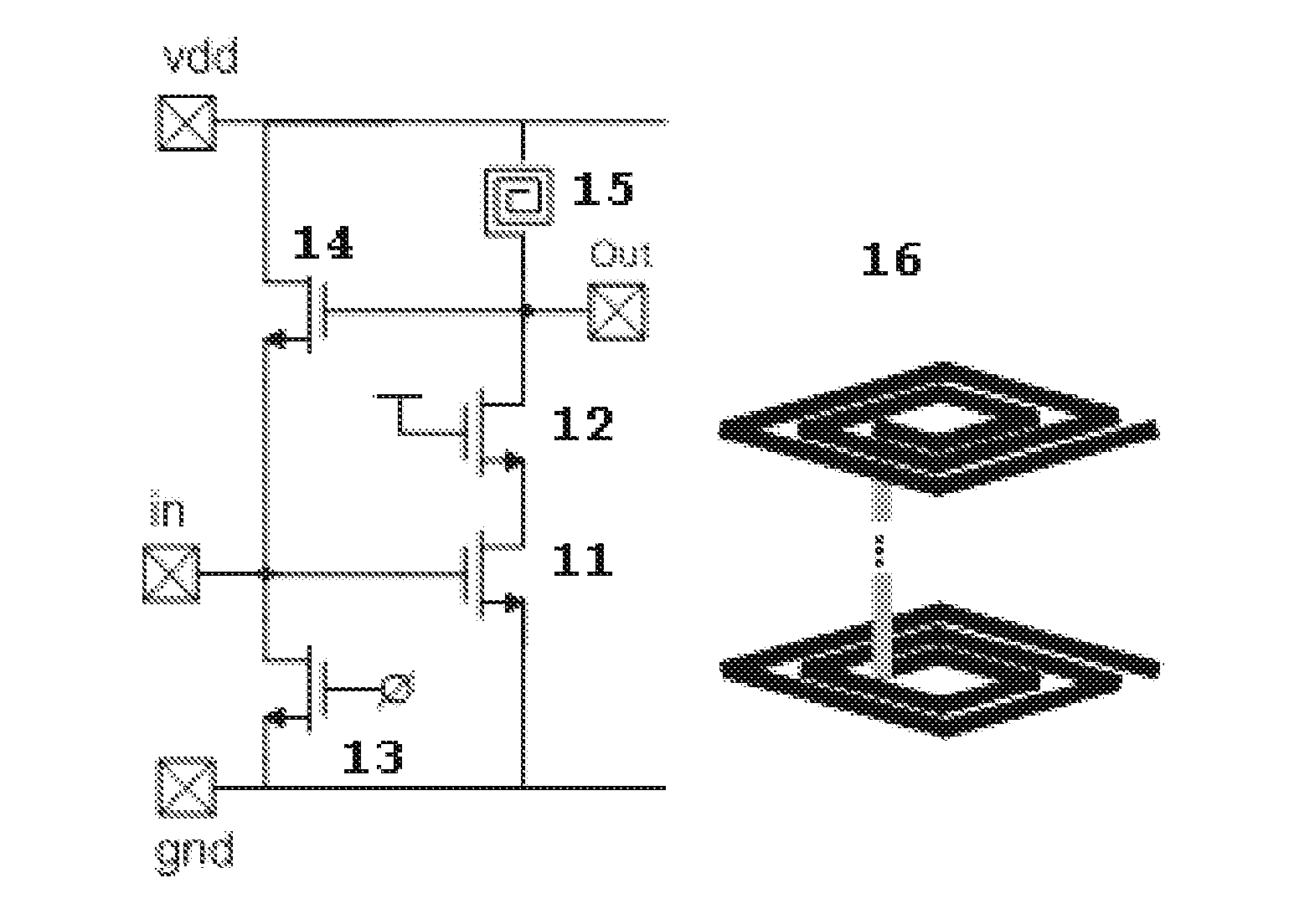
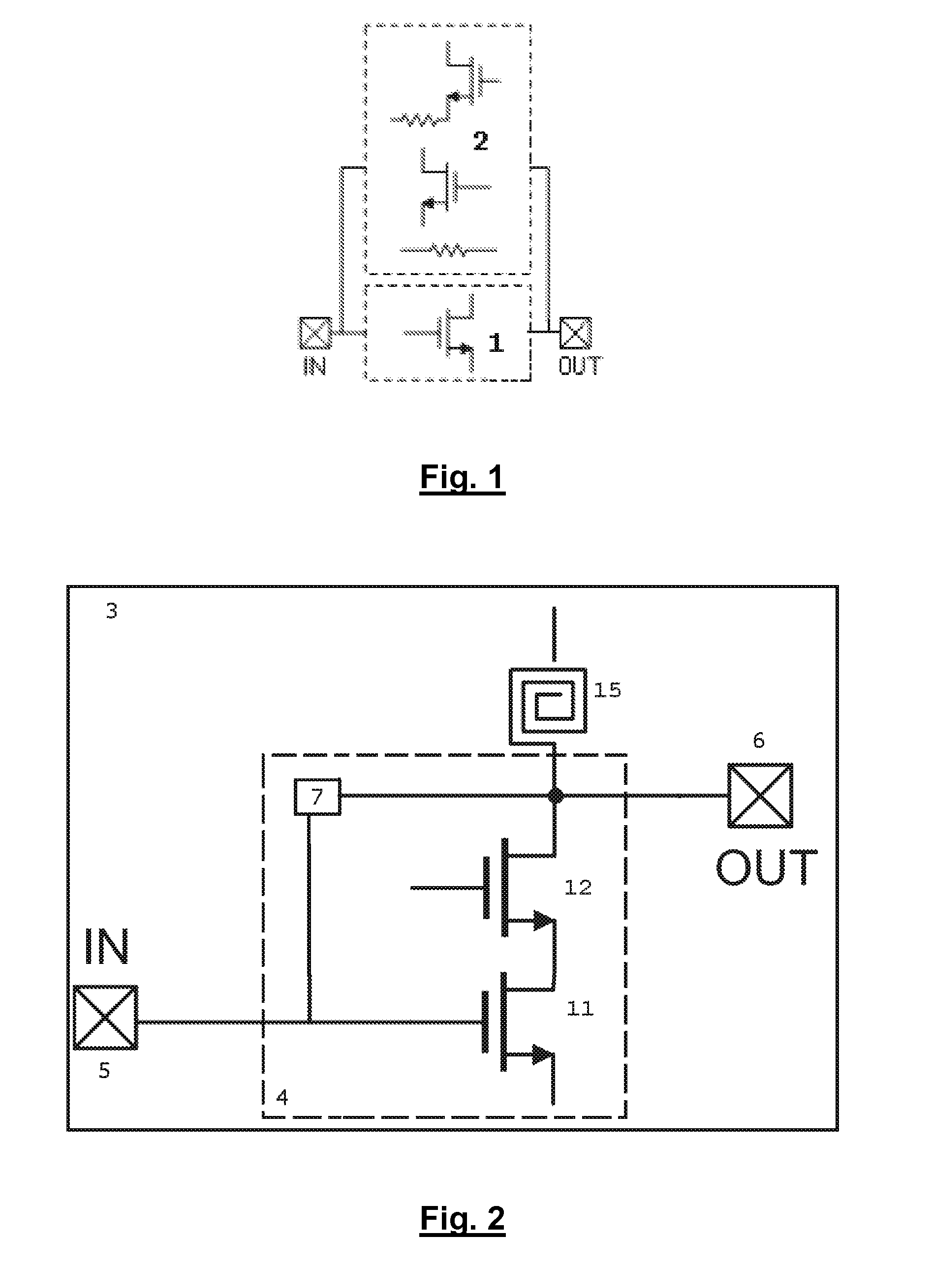
[0038]FIG. 1 shows a design comprising an amplifier (1) and a feedback amplifier (2). This design is known in...


PUM


Abstract

A low noise amplifying (LNA) circuit comprising an amplifying section (11, 12) and a feedback means (14) arranged for providing input matching from the output to the input. The LNA circuit further comprises at least one frequency band determining inductor (15) having a predetermined resonance frequency for influencing at least one frequency band in which the amplifying section operates. The at least one inductor is directly connected to the output of the circuit and the feedback means (14) provides a feedback connection for the section (s) to the input. In this way, the at least one frequency band in which the amplifying section operates is substantially completely determined by the at least one frequency band determining inductor (15).

Description

TECHNICAL FIELD[0001]The present invention relates to a low area LNA technique applicable for switched multiband LNA design, particular in digital CMOS.BACKGROUND ART[0002]Nowadays, multistandard and software-defined radios are emerging, encouraged by the RF capabilities of scaled CMOS and ultimately striving for cognitive radios. Meanwhile, the mask costs of scaled CMOS rise to dramatic heights. In a search for ways to repay this increased cost, low area RF design in digital CMOS has become a hot research topic.[0003]Broadband amplifiers are commonly used as a low area solution for the integration of LNAs for multistandard receivers, as in R. Bagheri et al., “An 800-MHz-6-GHz Software-Defined Wireless Receiver in 90-nm CMOS”, IEEE JSSC, Vol. 41, No. 12, pp. 2860-2876, December 2006. In scaled CMOS technologies, inductor-less designs attain bandwidths above 6 GHz. Their broadband nature however, imposes high linearity demands on both the LNA and at system level. Alternatively, separ...

Claims


Application Information

Patent Timeline
Patent Type & Authority Applications(United States)
IPC IPC(8): H03F1/34H03F1/22
CPCH03F1/223H03F2203/7209H03F1/42H03F1/56H03F3/195H03F3/72H03F2200/111H03F2200/151H03F2200/222H03F2200/294H03F2200/306H03F2200/378H03F2200/429H03F2200/451H03F1/342
Inventor BORREMANS, JONATHAN
Owner INTERUNIVERSITAIR MICRO ELECTRONICS CENT (IMEC VZW)
Why Eureka
Try Eureka