Semiconductor laser device

Active Publication Date: 2010-12-02
SHARP FUKUYAMA LASER CO LTD
View PDF5 Cites 1 Cited by
  • Summary
  • Abstract
  • Description
  • Claims
  • Application Information

AI Technical Summary

Benefits of technology

[0020]According to the present invention, the wavelength dependence of the monitor current is small and specifications capable of APC

Problems solved by technology

In 400 nm-range semiconductor laser devices, which are for the next generation Blu-ray disks, however, the temperature dependence of semiconductor laser devices causes the wavelength of an output laser to grow longer as the ambient temperature rises, despite laser power being kept constant.
The resultant problem is wild fluctuations in monitor current detected by the photodio

Method used


Image

  • Semiconductor laser device
  • Semiconductor laser device
  • Semiconductor laser device

Examples


Embodiment Construction

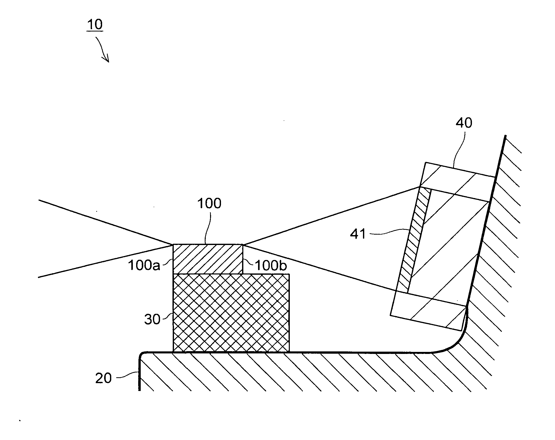
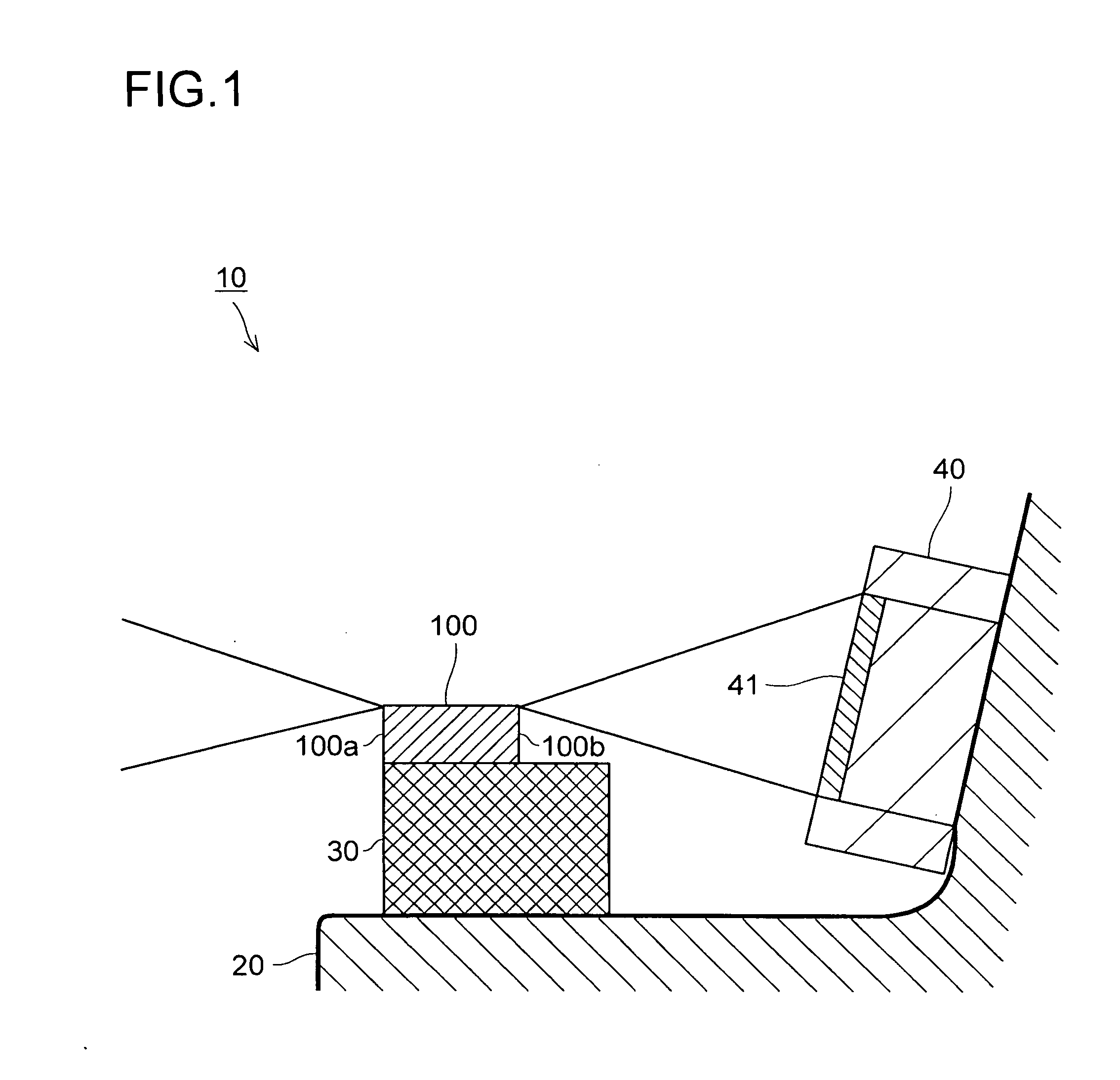
[0037]FIG. 1 is a sectional view of a main part of a semiconductor laser device according to the present invention. A semiconductor laser device 10 includes a stem 20, which has a horizontal surface for mounting a chip and a slanted surface, a sub-mount 30, which is placed on the horizontal surface of the stem 20, a semiconductor laser chip 100, which is placed on the sub-mount 30, and a photodiode 40, which is placed on the slanted surface of the stem 20.

[0038]The semiconductor laser chip 100 has an emission surface 100a and a reflection surface 100b, which are the opposing end surfaces of a resonator. The photodiode 40 is provided on the side of the reflection surface 100b to detect light that exits the reflection surface 100b with a light receiving part 41 thereof. The structure of the semiconductor laser chip 100 and a method of manufacturing the semiconductor laser chip 100 are described next.

[0039](Laser Wafer Fabrication)

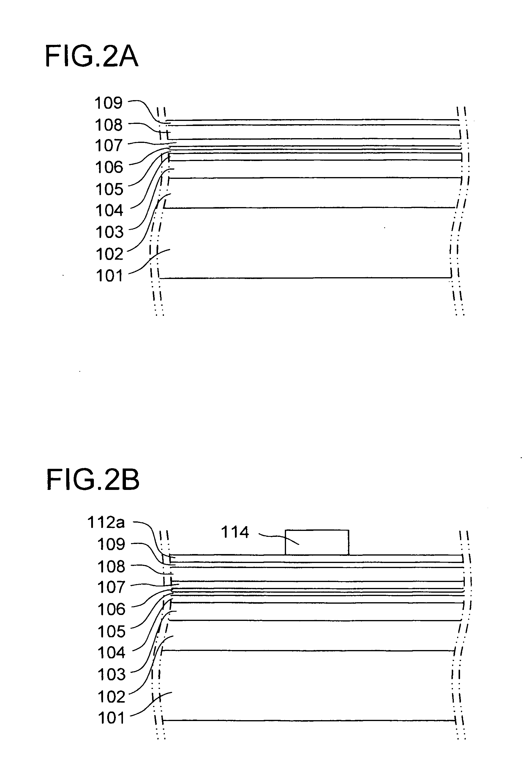
[0040]FIGS. 2A and 2B and FIGS. 3A to 3C are diagrams i...


PUM


Abstract

A semiconductor laser device has structure including: a semiconductor laser chip having an emission surface and a reflection surface which are opposing end surfaces of a resonator; and a photodiode for detecting light that exits from the reflection surface side, the photodiode being used in a wavelength band where a sensitivity of the photodiode rises as a wavelength lengthens, in which the emission surface has a first dielectric multilayer film formed thereon and the reflection surface has a second dielectric multilayer film formed thereon, and in which, when a wavelength at which a reflectance of the first dielectric multilayer film peaks is given as λf and a wavelength at which a reflectance of the second dielectric multilayer film peaks is given as λr, a relation λfr is satisfied.

Description

[0001]The present application claims priority from Japanese Patent Application No. 2009-127207 filed on May 27, 2009, the content of which is hereby incorporated by reference into this application.BACKGROUND OF THE INVENTION[0002]1. Field of the Invention[0003]The present invention relates to a semiconductor laser device including a semiconductor laser chip in which coating films are formed for an emission surface and a reflection surface, which are opposing end surfaces of a resonator.[0004]2. Description of Related Art[0005]A semiconductor laser element used in an optical disk drive generally includes a built-in photodiode for detecting laser power, in addition to a semiconductor laser chip, and laser power is controlled based on a current value (monitor current) converted by the photodiode through photoelectric effect. Inexpensive photodiodes which use silicon (Si) have conventionally been employed in 780 nm-range semiconductor laser elements for CDs and 650 nm-range semiconducto...

Claims


Application Information

Patent Timeline
IPC IPC(8): H01S5/026
CPCB82Y20/00H01S5/0202H01S5/02252H01S5/0287H01S5/0683H01S5/2009H01S5/22H01S5/34333H01S5/1221H01S5/02326
Inventor SOGABE, RYUICHI
Owner SHARP FUKUYAMA LASER CO LTD
Why Eureka
Try Eureka