Method and apparatus for etching

a technology of etching and apparatus, applied in the direction of microstructural technology, microstructural device, electric discharge tube, etc., can solve the problems of limited power capacity, difficult to achieve good etching uniformity in larger substrate formats, and small plasma generation area of typical rie reactors. achieve the effect of higher bias power

Inactive Publication Date: 2010-12-09
APPLIED MATERIALS INC
View PDF5 Cites 22 Cited by
  • Summary
  • Abstract
  • Description
  • Claims
  • Application Information

AI Technical Summary

Benefits of technology

[0012]In some embodiments, etching the substrate using a gas mixture including a fluorine-containing gas and oxygen is performed at a higher bias power than etching a silicon-containing layer the substrate using a fluorine-containing gas without mixing oxygen.

Problems solved by technology

The demand for Micro-Electro-Mechanical Systems (MEMS) devices has introduced new challenges for processing equipment companies.
One challenge is providing equipment suitable for efficient plasma etching of materials utilized to fabricate MEMS structures.
Typical RIE reactors generally have limited small plasma generation areas and limited power capability.
This makes it difficult to achieve good etching uniformity in larger substrate formats and also limits the etch rate.
Moreover, RIE reactors generally etch faster in the center relative the edge of a substrate, which limits potential product yields and quality.
Poor control of the cyclical etch process disadvantageously increases the roughness of the sidewalls, which may render a microelectronic device defective.

Method used


Image

  • Method and apparatus for etching
  • Method and apparatus for etching
  • Method and apparatus for etching

Examples


Embodiment Construction

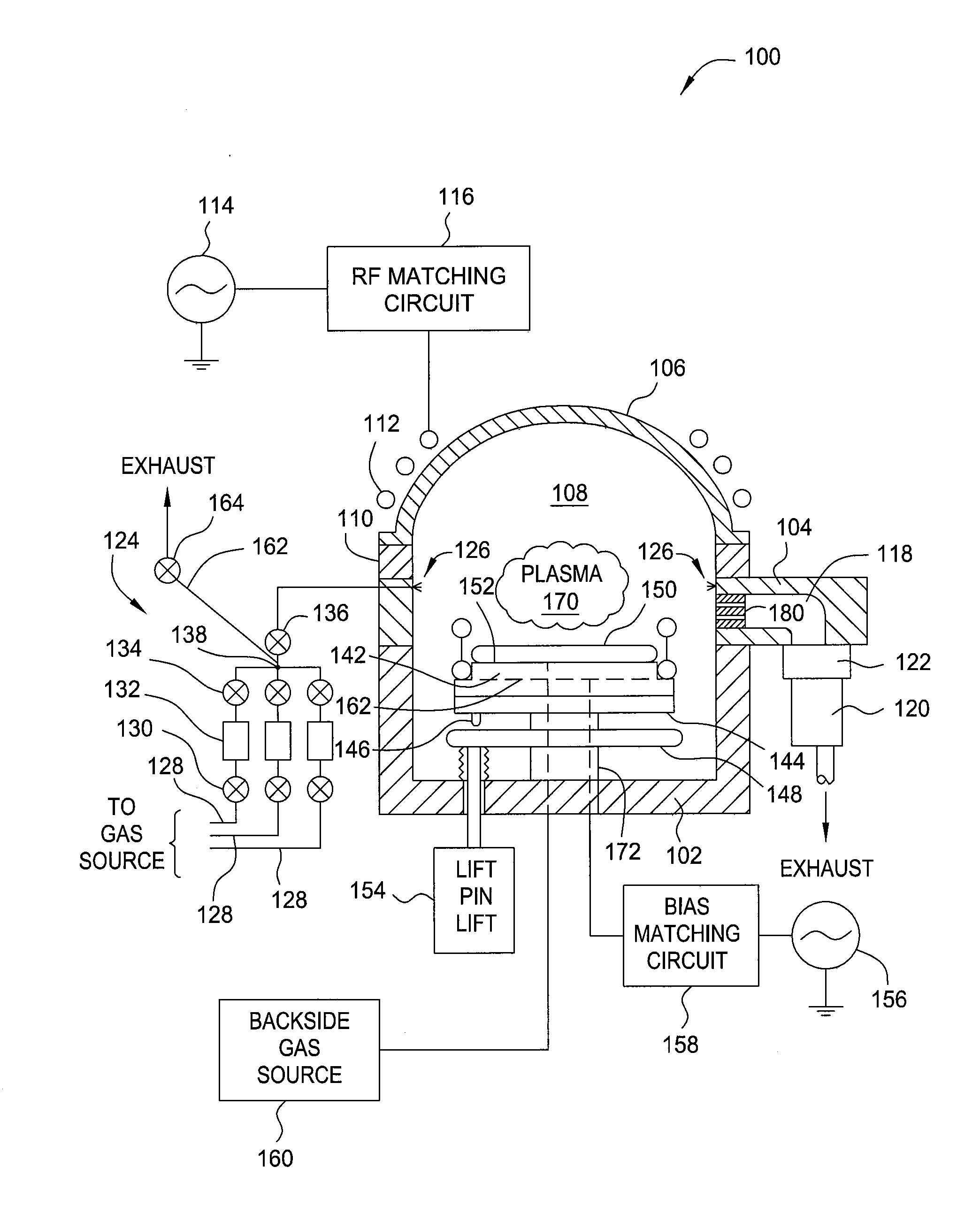
[0021]The invention generally relates to an apparatus and method of for etching. Although the apparatus and methods described herein are particularly advantageous for etching silicon for MEMS applications, it is contemplated that the embodiments of the invention are not limited to use with silicon etching, but may be beneficially utilized to etch other types of materials and / or be utilized in other etch reactors. To better understand the novelty of the apparatus of the invention and the methods of use thereof, reference is hereafter made to the accompanying drawings.

[0022]FIG. 1 is a sectional view of one embodiment of an etch reactor 100. The etch reactor 100 includes a lower chamber body 102, an upper chamber body 104, and a ceiling 106 which enclose a process volume 108. The ceiling 106 may be flat or have other geometry. In one embodiment, the ceiling 106 is a dome. An interchangeable spacer 110 is provided between the ceiling 106 and the upper chamber body 104 so that the incli...


PUM

PropertyMeasurementUnit
radio frequencyaaaaaaaaaa
lengthaaaaaaaaaa
frequencyaaaaaaaaaa

Abstract

Embodiments of the invention relate to a substrate etching method and apparatus. In one embodiment, a method for etching a substrate in a plasma etch reactor is provided that includes a) depositing a polymer on a substrate in an etch reactor, b) etching the substrate using a gas mixture including a fluorine-containing gas and oxygen in the etch reactor, c) etching a silicon-containing layer the substrate using a fluorine-containing gas without mixing oxygen in the etch reactor, and d) repeating a), b) and c) until an endpoint of a feature etched into the silicon-containing layer is reached.

Description

CROSS-REFERENCE TO RELATED APPLICATIONS[0001]This application claims benefit of U.S. Provisional Patent Application Ser. No. 61 / 183,604, filed Jun. 3, 2009, which is incorporated by reference in its entirety.BACKGROUND OF THE INVENTION[0002]1. Field of the Invention[0003]Embodiments of the invention generally relate a method and apparatus for etching, and more particularly, a method and apparatus suitable for etching Micro-Electro-Mechanical Systems (MEMS) devices and the like.[0004]2. Description of the Related Art[0005]The demand for Micro-Electro-Mechanical Systems (MEMS) devices has introduced new challenges for processing equipment companies. One challenge is providing equipment suitable for efficient plasma etching of materials utilized to fabricate MEMS structures. For example, processing equipment utilized for etching must be able to maintain good critical dimension control and mask selectivity in order to successfully manufacture MEMS structures on a commercially viable sca...

Claims


Application Information

Patent Timeline
Patent Type & Authority Applications(United States)
IPC IPC(8): C23F1/00
CPCB81C1/00531B81C2201/0112H01L21/30655H01J37/3244H01J37/32449H01J37/321C23F4/04H01L21/3065
Inventor CHESHIRE, ALAN
Owner APPLIED MATERIALS INC
Why Eureka
Try Eureka