Reflection-type photomasks and methods of fabricating the same

Active Publication Date: 2013-08-01
SK HYNIX INC
View PDF1 Cites 7 Cited by
  • Summary
  • Abstract
  • Description
  • Claims
  • Application Information

AI Technical Summary

Benefits of technology

[0032]In various embodiments, the trench may be formed by alternately and repeatedly applying a first etch process and a second etch process to the reflection layer. I

Problems solved by technology

Even though the lights having short wavelengths such as the i-line beam, the KrF laser beam and the ArF laser beam are used in the exposure step of the photolithography process, there may be still limitations in enhancing the pattern resolutions of the highly integrated semiconductor devices.
However, the EUV ray may have high energy because the wavelength of the E

Method used


Image

  • Reflection-type photomasks and methods of fabricating the same
  • Reflection-type photomasks and methods of fabricating the same
  • Reflection-type photomasks and methods of fabricating the same

Examples


Embodiment Construction

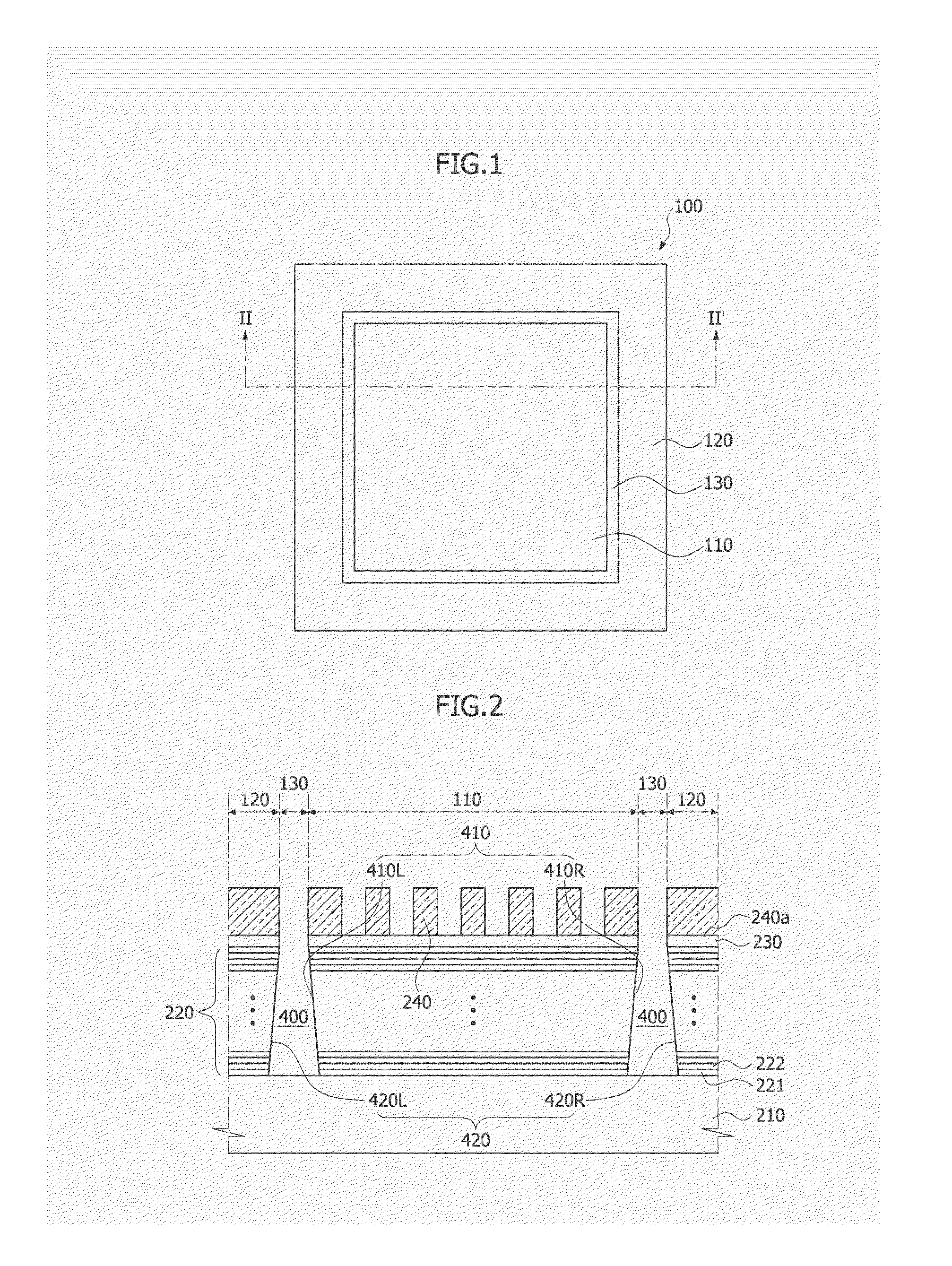
[0040]FIG. 1 is a plan view illustrating a reflection-type photomask according to various embodiments, and FIG. 2 is a cross sectional view taken along a line II-II′ of FIG. 1. Referring to FIGS. 1 and 2, a reflection-type photomask 100 according to an embodiment may include a pattern transfer region 110 having image patterns corresponding to patterns which may be formed on a wafer, a light blocking region120 surrounding the pattern transfer region 110, and a border region 130 disposed between the pattern transfer region 110 and the light blocking region 120. The pattern transfer region 110 may be configured to include a substrate 210, a reflection layer 220 disposed on a surface of the substrate 210, a capping layer 230 disposed on a surface of the reflection layer 220 opposite to the substrate 210, and first absorption layer patterns 240 disposed on a surface of the capping layer 230 opposite to the reflection layer 220 to expose portions of the capping layer 230. The light blocki...


PUM


Abstract

Reflection-type photomasks are provided. The reflection-type photomask includes a substrate and a reflection layer on a front surface of the substrate. The substrate includes a pattern transfer region, a light blocking region and a border region. A trench penetrates the reflection layer in the border region to expose the substrate. First absorption layer patterns are disposed on the reflection layer in the pattern transfer region, and a second absorption layer pattern is disposed on the reflection layer in the light blocking region. Sidewalls of the trench have a sloped profile. Related methods are also provided.

Description

CROSS-REFERENCES TO RELATED APPLICATIONS[0001]The present application claims priority under 35 U.S.C 119(a) to Korean Application Nos. 10-2012-0009198 and 10-2012-0150090, filed on Jan. 30, 2012 and Dec. 20, 2012, respectively, in the Korean intellectual property Office, which are incorporated herein by references in their entirety as set forth in full.BACKGROUND[0002]1. Technical Field[0003]Embodiments of the present disclosure generally relate to photomasks used in fabrication of semiconductor devices and methods of fabricating the photomasks and, more particularly, to reflection-type photomasks used in fabrication of semiconductor devices and methods of fabricating the reflection-type photomasks.[0004]2. Related Art[0005]Integration density of semiconductor devices has been continuously increased with the development of a nano-technology. As the semiconductor devices become more highly integrated, some elements such as transistors and interconnection lines have been scaled down t...

Claims


Application Information

Patent Timeline
IPC IPC(8): G03F1/24
CPCG03F1/24
Inventor RYU, CHOONG HANKIM, YONG DAE
Owner SK HYNIX INC
Why Eureka
Try Eureka