Load reduced memory module and memory system including the same

a memory module and load reduction technology, applied in the field of memory modules and memory systems, can solve the problems of increasing the capacity of a data line on the motherboard, reducing signal quality, and difficult to provide the required memory capacity with a single memory module, and achieves the effects of enhancing signal quality, reducing the length of the line between the data register buffer and the memory chip, and enhancing signal quality

Active Publication Date: 2010-12-09
LONGITUDE LICENSING LTD
View PDF27 Cites 36 Cited by
  • Summary
  • Abstract
  • Description
  • Claims
  • Application Information

AI Technical Summary

Benefits of technology

[0012]According to the present invention, because a plurality of data register buffers are mounted on a module PCB and a command/address/control register buffer is mounted on the module PCB separately from the data register buffers, a line length between a data regis

Problems solved by technology

In recent years, because a system requires a considerable amount of memory capacity, it is hard to provide the required memory capacity with a single memory module.
However, when a plurality of memory modules are mounted on a motherboard, a load capacity of a data line on the motherboard increases, resulting in a degradation of signal quality.
Although it does not cause a serious problem when a data transfer rate between the memory controller and the memory module is relatively low, it may cause a serious problem that the data transfer cannot be performed in a proper manner due to the degradation of the signal quality when the data transfer rate increases to a certain level.
However, because the AMB employed in the Fully

Method used


Image

  • Load reduced memory module and memory system including the same
  • Load reduced memory module and memory system including the same
  • Load reduced memory module and memory system including the same

Examples


Embodiment Construction

[0041]Preferred embodiments of the present invention will be explained below in detail with reference to the accompanying drawings.

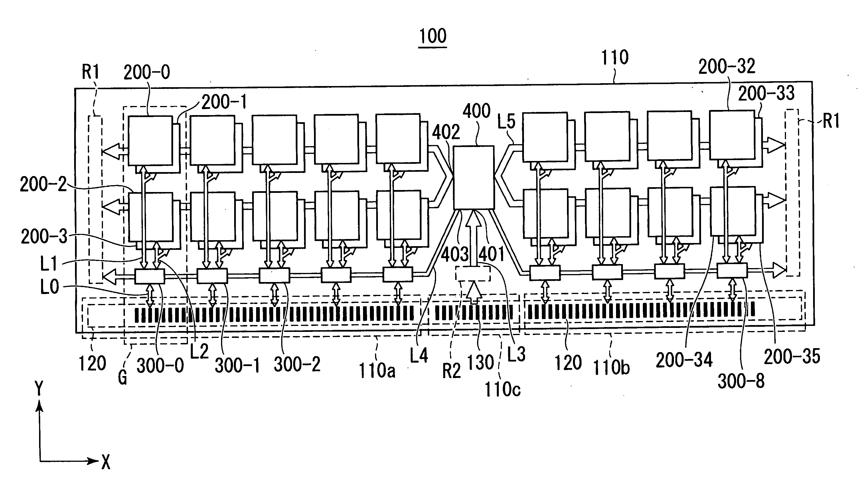
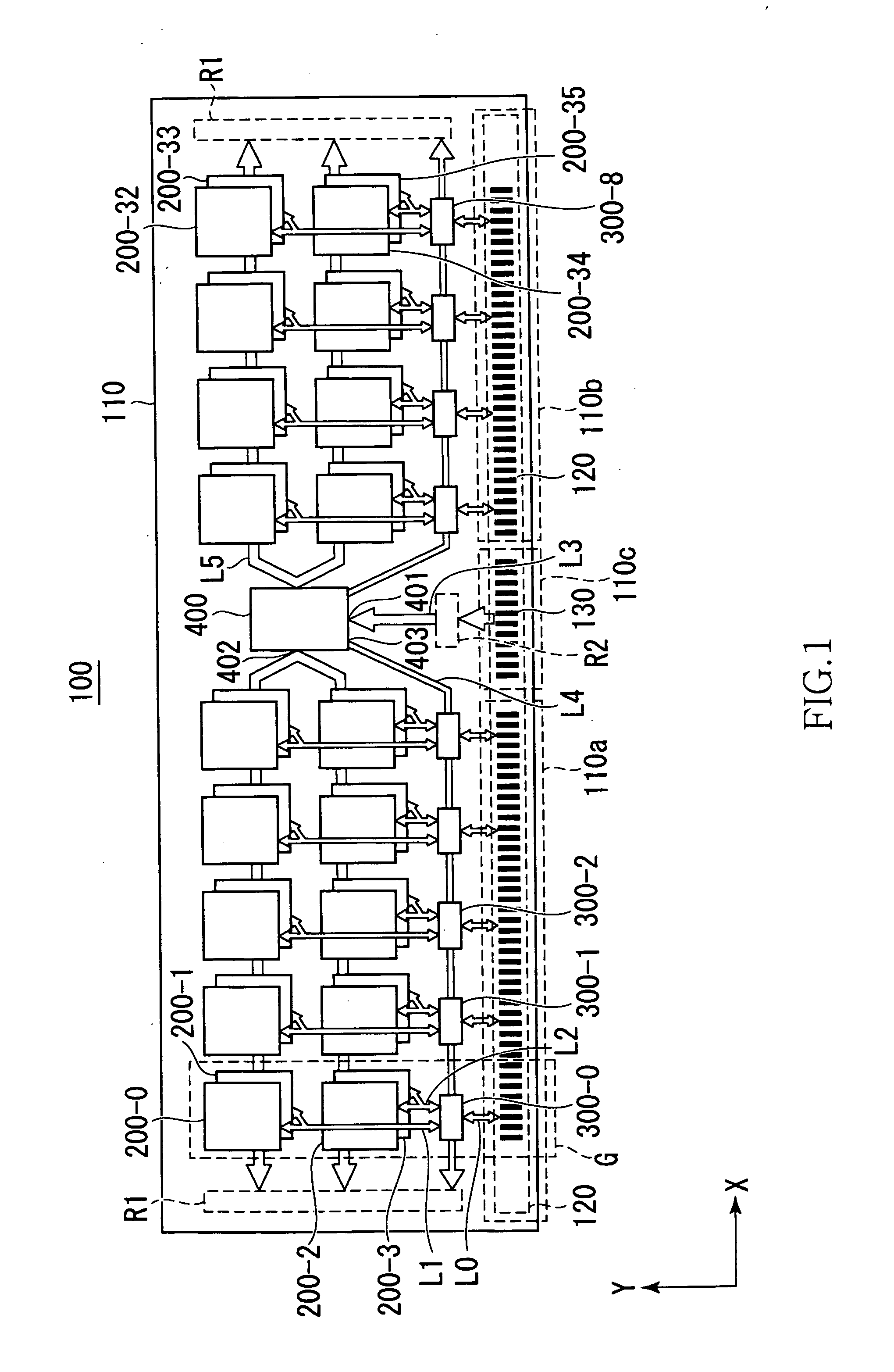
[0042]FIG. 1 is a schematic diagram of a configuration of a memory module 100 according to an embodiment of the present invention.

[0043]As shown in FIG. 1, the memory module 100 according to the present embodiment includes a module PCB 110, a plurality of memory chips 200 mounted on the module PCB 110, a plurality of data register buffers 300, and a command / address / control register buffer 400.

[0044]In the present embodiment, the memory module 100 includes thirty-six memory chips 200. When it is necessary to specify each of the memory chips, the memory chips are respectively represented by memory chips 200-0 to 200-35. Furthermore, in the present embodiment, the memory module 100 includes nine data register buffers 300. When it is necessary to specify each of the data register buffers, the data register buffers are respectively represented by data registe...


PUM


Abstract

A memory module includes a plurality of memory chips, a plurality of data register buffers, and a command/address/control register buffer mounted on a module PCB. The data register buffers perform data transfers with the memory chips. The command/address/control register buffer performs buffering of a command/address/control signal and generates a control signal. The buffered command/address/control signal is supplied to the memory chips, and the control signal is supplied to the data register buffers. According to the present invention, because line lengths between the data register buffers and the memory chips are shortened, it is possible to realize a considerably high data transfer rate.

Description

BACKGROUND OF THE INVENTION[0001]1. Field of the Invention[0002]The present invention relates to a memory module and a memory system including the same, and more particularly relates to a Load Reduced memory module and a memory system including the same.[0003]2. Description of Related Art[0004]A memory module such as a DIMM (Dual Inline Memory Module) has a configuration in which a large number of memory chips such as DRAMs (Dynamic Random Access Memories) are mounted on a module printed circuit board (PCB). Such a memory module is inserted in a memory slot provided on a motherboard, thereby a data transfer is performed between a memory controller and the memory module. In recent years, because a system requires a considerable amount of memory capacity, it is hard to provide the required memory capacity with a single memory module. Therefore, in most cases, the motherboard includes a plurality of memory slots, so that a plurality of memory modules can be mounted on the motherboard.[...

Claims


Application Information

Patent Timeline
IPC IPC(8): G11C5/02G11C7/00
CPCG11C5/04G11C5/063G11C7/10G11C7/1051G11C7/00G11C7/1078G11C7/1087G11C7/109G11C5/02G11C7/106H01L2224/48091H01L2224/48227H01L2924/15311H01L2924/00014
Inventor SAITO, SHUNICHISUGANO, TOSHIOHIRAISHI, ATSUSHIOSANAI, FUMIYUKINAKAMURA, MASAYUKIFUJISAWA, HIROKI
Owner LONGITUDE LICENSING LTD
Why Eureka
Try Eureka