Horizontally depleted metal semiconductor field effect transistor

a metal semiconductor and field effect technology, applied in the field of horizontal depletion metal semiconductor field effect transistors, can solve the problems of continuous reduction in the thickness of the silicon layer, undesired performance variability, and the failure of mesfet b>10/b> to perform as desired

Inactive Publication Date: 2010-12-23
ARIZONA STATE UNIVERSITY
View PDF7 Cites 13 Cited by
  • Summary
  • Abstract
  • Description
  • Claims
  • Application Information

AI Technical Summary

Problems solved by technology

Unfortunately, the continuous pressure to reduce component sizes and increase integration has led to a continual reduction in the thickness of the silicon layer 30 in which MESFETs and other devices are formed.
Even when sufficient silicon remains beneath the gate contact 20 for the channel region 12, the relative variability of the thickness tc of the channel region 12 results in undesired performance variability.
Second, even if the depth of the gate contact 20 could be tightly controlled, the MESFET 10 will not perform as desired once the thickness tc of the channel region 12 becomes too small.

Method used


Image

  • Horizontally depleted metal semiconductor field effect transistor
  • Horizontally depleted metal semiconductor field effect transistor
  • Horizontally depleted metal semiconductor field effect transistor

Examples


Embodiment Construction

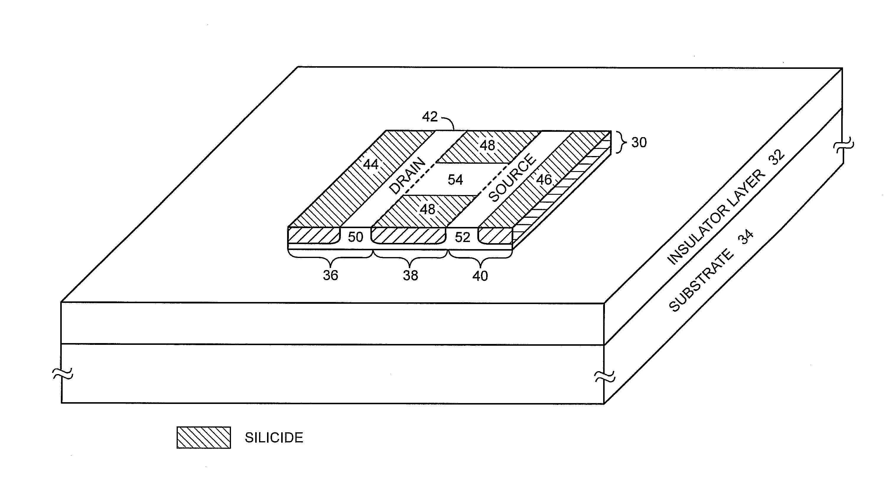
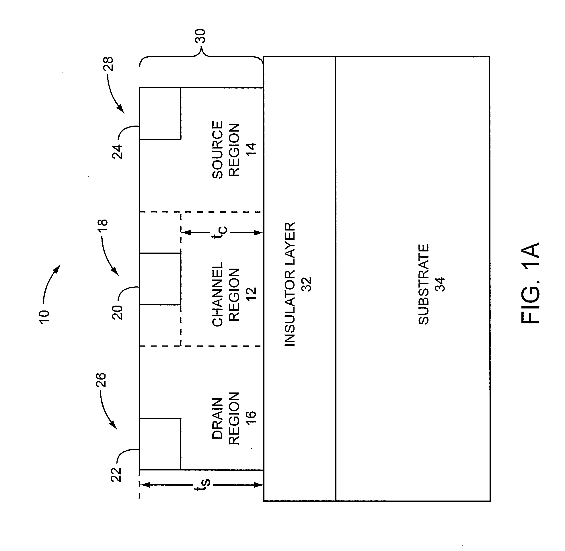
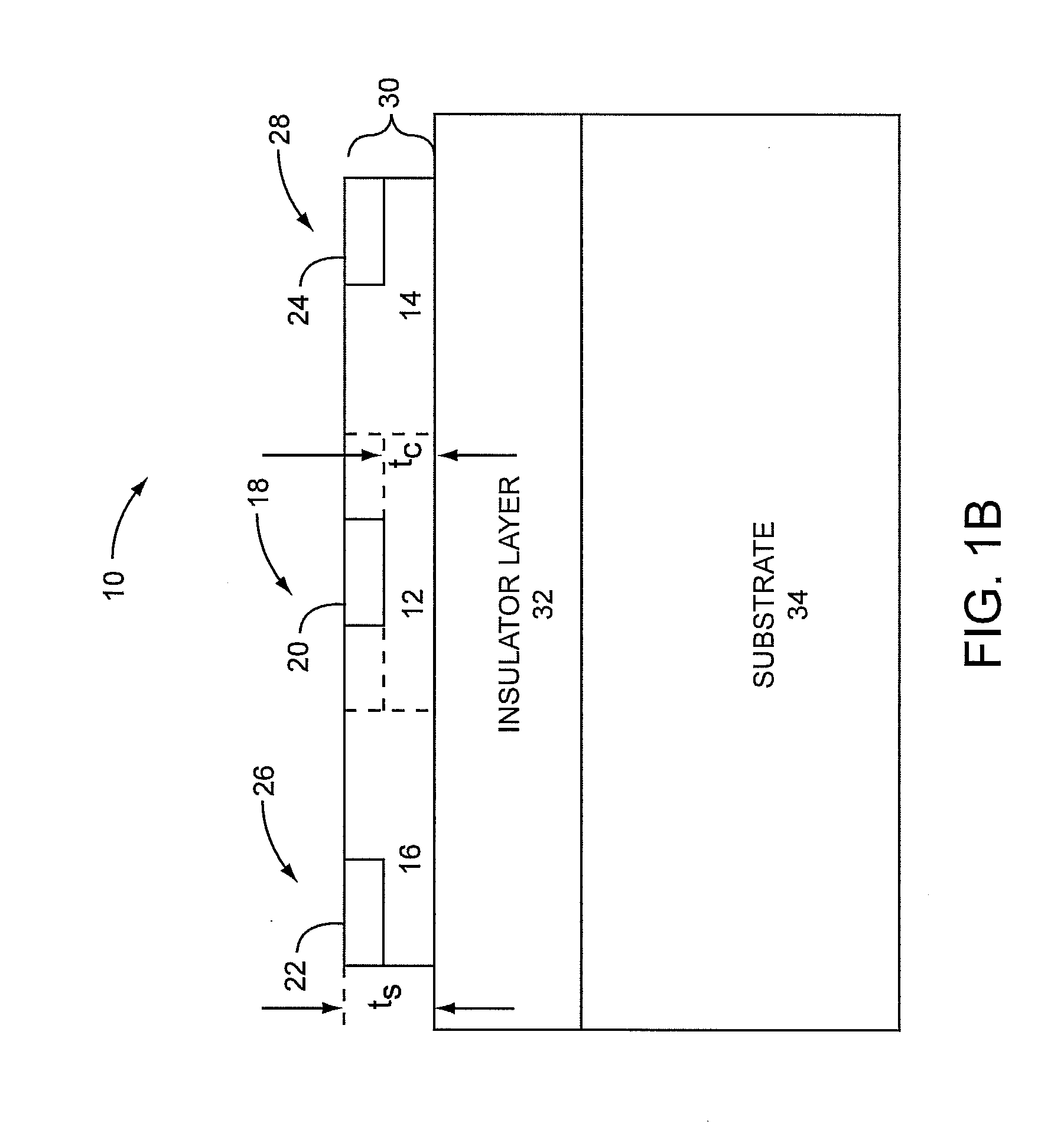
[0029]The embodiments set forth below represent the necessary information to enable those skilled in the art to practice the invention and illustrate the best mode of practicing the invention. Upon reading the following description in light of the accompanying drawing figures, those skilled in the art will understand the concepts of the invention and will recognize applications of these concepts not particularly addressed herein. It should be understood that these concepts and applications fall within the scope of the disclosure and the accompanying claims. Notably, the terms “inner” and “outer” are used herein to identify relative portions of various sections or regions relative to the center of an overall device or module.

[0030]The present invention relates to a Metal Semiconductor Field Effect Transistor (MESFET) architecture that can be formed in seamless processes that employ relatively thin silicon device layers. While traditional MESFETs typically employ a horizontal depletio...


PUM


Abstract

The present invention provides a horizontally depleted Metal Semiconductor Field Effect Transistor (MESPET). A drain region, a source region, and a channel region are formed in the device layer such that the drain region and the source region are spaced apart from one another and the channel region extends between the drain region and the source region. First and second gate contacts are formed in the device layer on either side of the channel region, and as such, the first and second gate contacts will also reside between opposing portions of the source and drain regions. With this configuration, voltages applied to the first and second gate contacts effectively control vertical depletion regions, which form on either side of the channel region.

Description

[0001]This application claims the benefit of U.S. provisional application Ser. No. 60 / 971,778 filed Sep. 12, 2007, the disclosure of which is incorporated herein by reference in its entirety.FIELD OF THE INVENTION[0002]The present invention relates to field effect transistors, and in particular to a horizontally depleted Metal Semiconductor Field Effect Transistor (MESFET).BACKGROUND OF THE INVENTION[0003]Metal Semiconductor Field Effect Transistors (MESFETs) are becoming more ubiquitous in modern electronics and are particularly applicable in high speed and high voltage analog and digital electronics applications. As illustrated in FIG. 1A, a typical MESFET 10 includes a channel region 12 that extends between a source region 14 and a drain region 16. A Schottky gate structure 18 includes a gate contact 20 that resides over the channel region 12 and between a source contact 24 that resides over the source region 14 and a drain contact 22 that resides over the drain region 16. The so...

Claims


Application Information

Patent Timeline
Patent Type & Authority Applications(United States)
IPC IPC(8): H01L29/812H01L21/338
CPCH01L29/1037H01L29/42316H01L29/66848H01L29/7855H01L2029/7857H01L29/7832H01L29/4238H01L29/47H01L29/8126H01L29/8124
Inventor ERVIN, JOSEPH E.THORNTON, TREVOR JOHN
Owner ARIZONA STATE UNIVERSITY
Why Eureka
Try Eureka