Semiconductor device

Inactive Publication Date: 2010-12-23
RENESAS ELECTRONICS CORP
View PDF0 Cites 14 Cited by
  • Summary
  • Abstract
  • Description
  • Claims
  • Application Information

AI Technical Summary

Benefits of technology

[0014]A first exemplary aspect of the present invention is a semiconductor including a memory cell including an information storage portion including an upper electrode layer and a lower electrode layer formed below the upper electrode layer and an access transistor for controlling access to the information storage portion, a bit-line connected to the access transistor to write or read data to or

Problems solved by technology

On the other hand, because the semiconductor device itself has been miniaturized, it becomes more difficult to secure an area for the decoupling capacitive element.
The Low-K material has a low dielectric constant so that the Low-K material is not suitable for a capacitance.
Further, since the Low-K material consumes wiring resources to the second metal line 2, it reduces the flexibility in terms of circuit connection usage, which is the original purpose of the wiring.
Therefore, no circuit can be formed on the area where the capacitive element is formed.
However, a withstand voltage of the capacitor of the DRAM cell is low.
Therefore, there is a problem in reliability when the DRAM cell is used as the decoupling capacitive element of the power supply in which a noise having an amplitude larger than the withstand voltage of the capacitor may occur.
Needless to say, the withstand voltage of the DRAM cell is too low to be used as the decoupling capacitive element of the power supply for a 3.3 V interface such as a USB.
That is, in a case where a capacitive element is formed in a semiconductor device including both of a DRAM circuit and a logic circuit, it is difficult to form a capacitive element that has a sufficient withstand voltage and capacitance while securing an area for forming the circuit.

Method used


Image

  • Semiconductor device
  • Semiconductor device
  • Semiconductor device

Examples


first exemplary embodiment

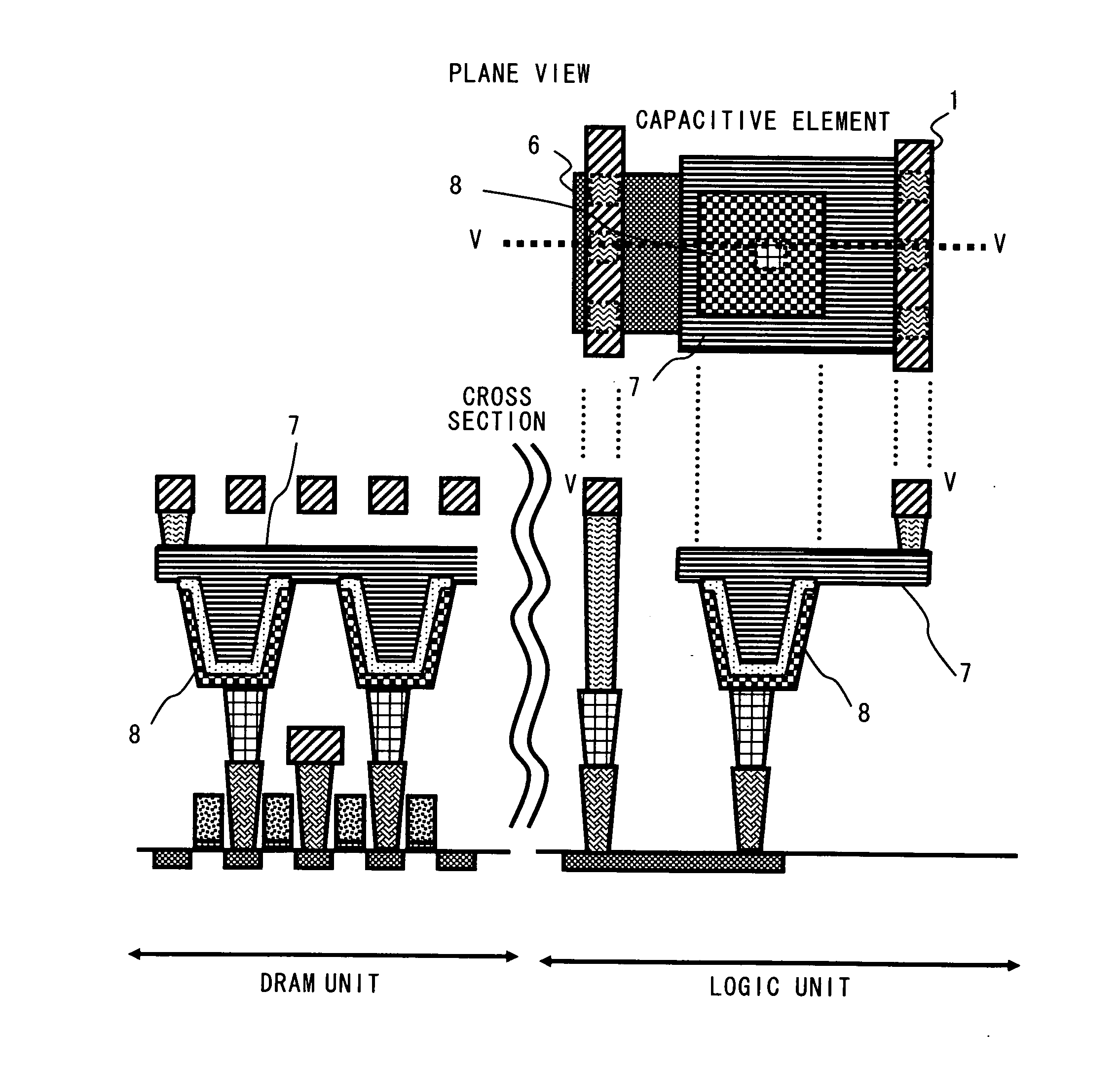
[0024]A semiconductor device according to the first exemplary embodiment of the present invention will be described with reference to FIG. 1. FIG. 1 shows a configuration of a semiconductor device according to a first exemplary embodiment. As shown in FIG. 1, the semiconductor device according to the first exemplary embodiment includes both of the DRAM unit and the logic unit.

[0025]In FIG. 1, a plane view of a parallel plate type capacitive element is shown on the upper side; a cross section of an area where the capacitive element of the DRAM unit is disposed is shown in a lower left part; and a cross section of an area where the capacitive element of the logic unit is disposed is shown in a lower right part. In the plane view of FIG. 1, components of the lower layers, which cannot be seen in reality, are also illustrated for the sake of explanation.

[0026]On the semiconductor substrate, a plurality of diffusion layers 11 are formed at predetermined intervals. On the semiconductor su...

second exemplary embodiment

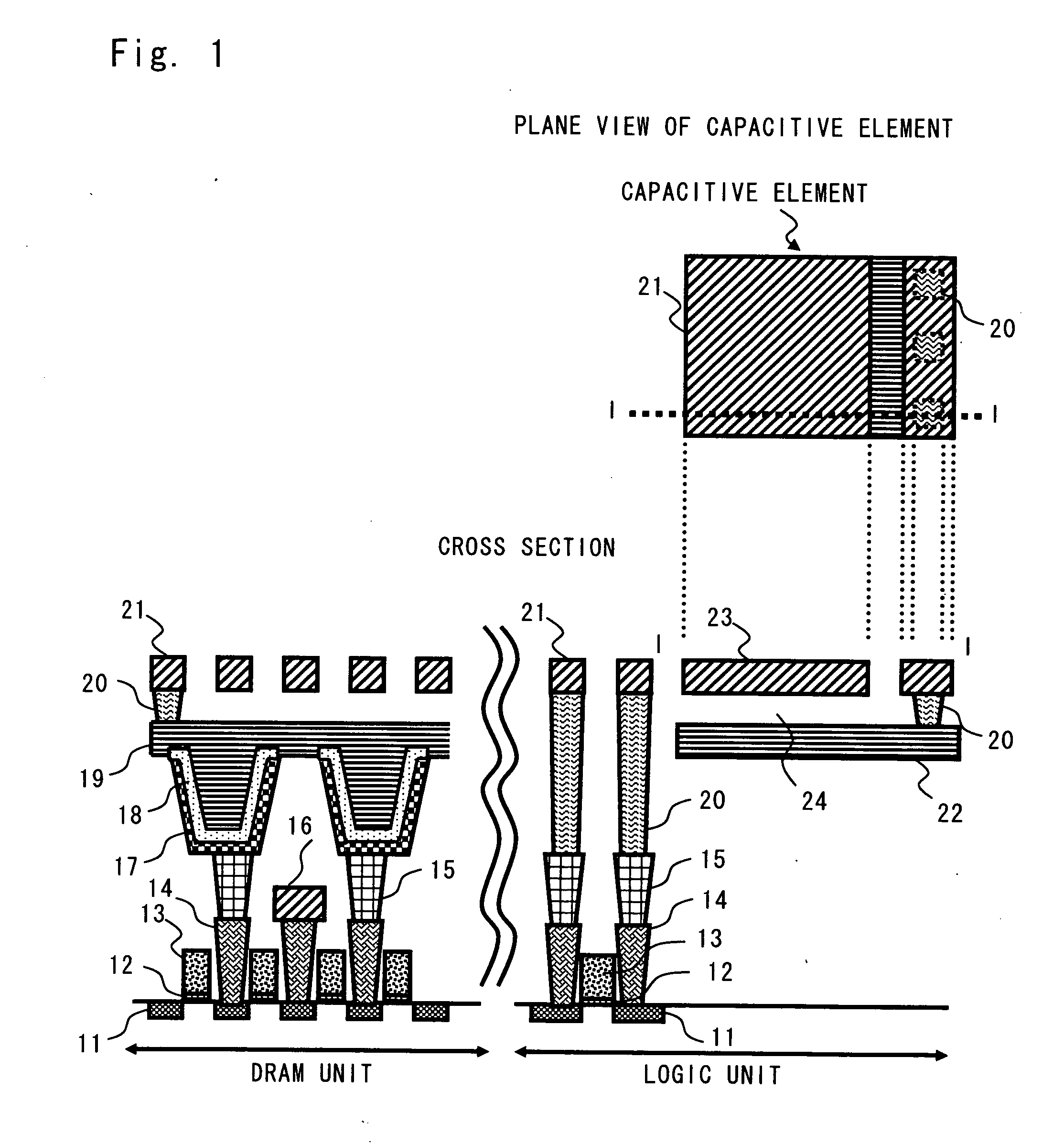
[0039]A semiconductor device according to a second exemplary embodiment of the present invention will be described with reference to FIG. 2. FIG. 2 shows a configuration of semiconductor device according to the second exemplary embodiment. In FIG. 2, the same components as those of FIG. 1 are denoted by the same reference symbols, and the description thereof is omitted.

[0040]In FIG. 2, a plane view of a parallel plate type capacitive element and a logic unit are shown on the upper side; a cross section of an area where the capacitive element of the DRAM unit is disposed is shown in a lower left part; and a cross section of an area where the capacitive element of the logic unit is disposed is shown in a lower right part. In the plane view of FIG. 2, components of the lower layers, which cannot be seen in reality, are also illustrated for the sake of explanation.

[0041]A semiconductor device according to the present exemplary embodiment includes, similarly to the first exemplary embodi...

third exemplary embodiment

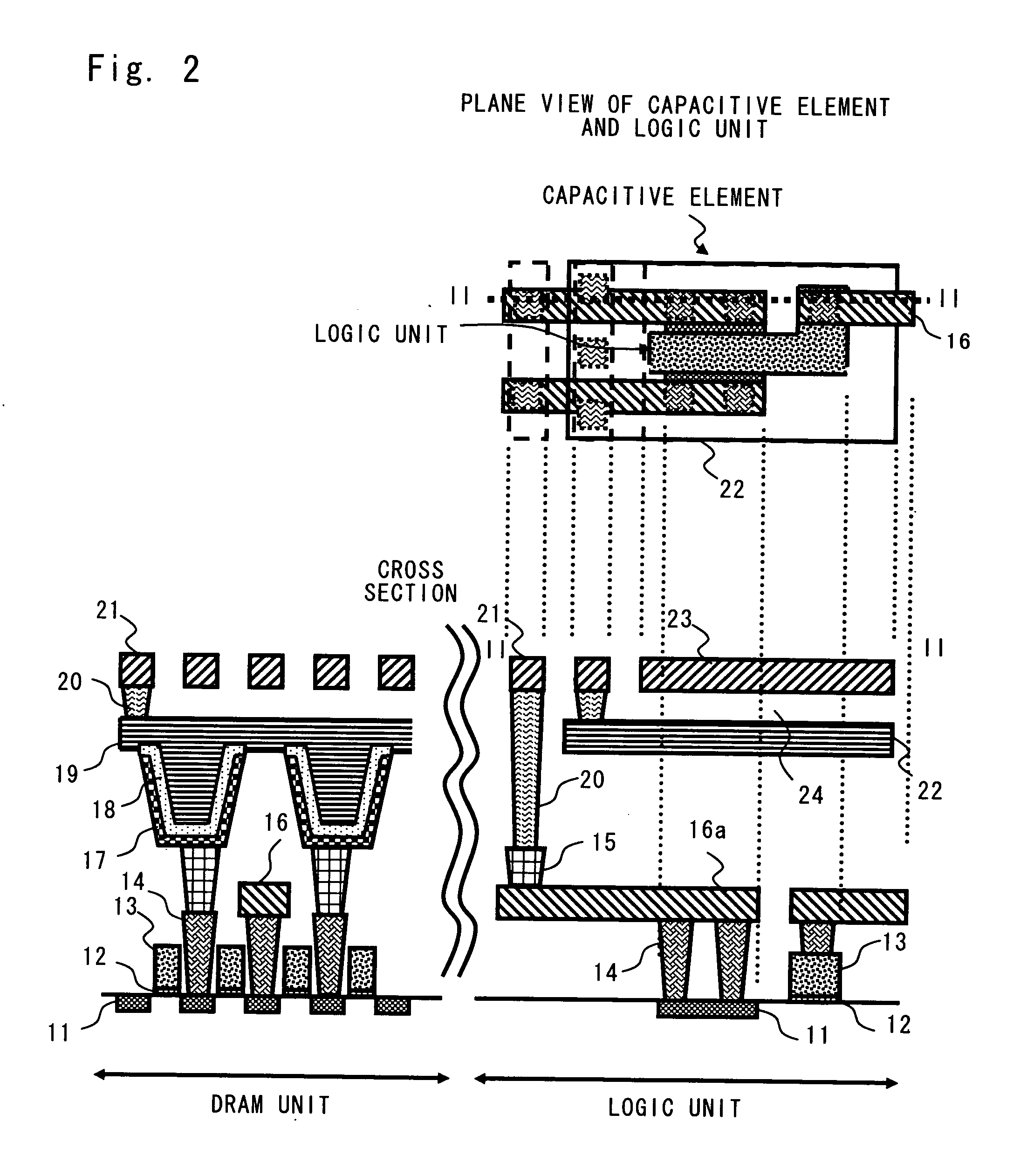
[0044]A semiconductor device according to a third exemplary embodiment of the present invention will be described with reference to FIG. 3. FIG. 3 shows a configuration of semiconductor device according to the third exemplary embodiment. In FIG. 3, the same components as those of FIGS. 1 and 2 are denoted by the same reference symbols, and the description thereof is omitted.

[0045]In FIG. 3, a plane view of a parallel plate type capacitive element and a gate capacitive element are shown on the upper side; a cross section of an area where the capacitive element of the DRAM unit is disposed is shown in a lower left part; and a cross section of an area where the capacitive element of the logic unit is disposed is shown in a lower right part. In the plane view of FIG. 3, components of the lower layers, which cannot be seen in reality, are also illustrated for the sake of explanation.

[0046]In the present exemplary embodiment, at the same horizontal position as the capacitive element inclu...


PUM


Abstract

A semiconductor device according to an exemplary embodiment of the present invention includes a memory cell including an information storage portion including a capacitor upper electrode of a DRAM cell and a capacitor lower electrode formed below the upper electrode and an access transistor for controlling access to the information storage portion, a bit-line connected to the access transistor to write or read data to or from the information storage portion, a word line connected to a gate electrode of the access transistor to control the access transistor, and a capacitive element including an upper electrode made from a same layer as a first metal line formed above the capacitor upper electrode and a lower electrode made from a same layer as the capacitor upper electrode, the capacitive element being formed outside an area where the memory cell is formed.

Description

INCORPORATION BY REFERENCE[0001]This application is based upon and claims the benefit of priority from Japanese patent application No. 2009-146179, filed on Jun. 19, 2009, the disclosure of which is incorporated herein in its entirety by reference.BACKGROUND[0002]1. Field of the Invention[0003]The present invention relates to a semiconductor device including both of a DRAM (Dynamic Random Access Memory) circuit and a logic circuit.[0004]2. Description of Related Art[0005]Recently, since the operation of a semiconductor device has become faster, the number of decoupling capacitive elements required to stabilize the high speed operation of the semiconductor device has increased. On the other hand, because the semiconductor device itself has been miniaturized, it becomes more difficult to secure an area for the decoupling capacitive element.[0006]For the sake of a finer design and lower power consumption of the device, a power supply voltage itself within the device has been decreasing...

Claims


Application Information

Patent Timeline
IPC IPC(8): H01L27/108
CPCH01L27/10814H01L27/10852H01L28/91H01L27/10897H01L27/10894H10B12/315H10B12/033H10B12/09H10B12/50
Inventor IZUMI, KATSUYA
Owner RENESAS ELECTRONICS CORP
Why Eureka
Try Eureka