Optical module

a technology of optical modules and optical elements, applied in the field of optical modules, can solve problems such as fluctuation of characteristics, and achieve the effect of reducing the stress applied to the packag

Active Publication Date: 2010-12-23
NIPPON TELEGRAPH & TELEPHONE CORP +1
View PDF5 Cites 24 Cited by
  • Summary
  • Abstract
  • Description
  • Claims
  • Application Information

AI Technical Summary

Benefits of technology

[0024]According to the fifth embodiment, the printed circuit board also can be made of aluminum nitride or silicon carbide having a thermal expansion coefficient close to that of silicon. Thus, even when a temperature fluctuation causes the PLC substrate to expand or contract to have a size fluctuation, the printed circuit board can move in accordance with the motion thereof expand or contract, thus reducing the stress applied to the package.

Problems solved by technology

The conventional optical module 1 had a disadvantage in that a temperature fluctuation tends to cause the fluctuation of a characteristic such as a light-receiving sensitivity characteristic.

Method used


Image

  • Optical module
  • Optical module
  • Optical module

Examples


embodiment 1

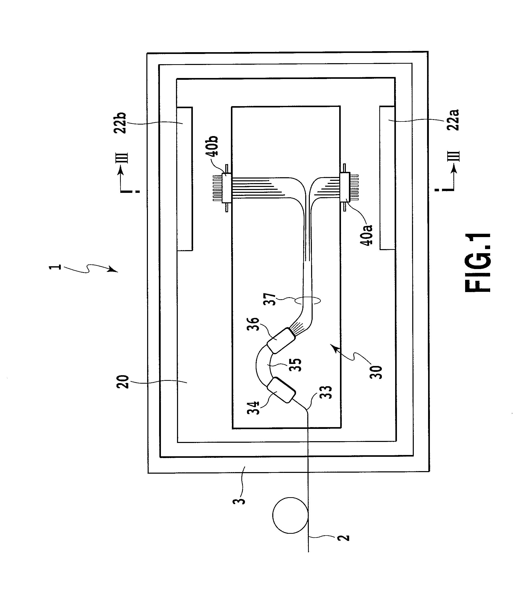
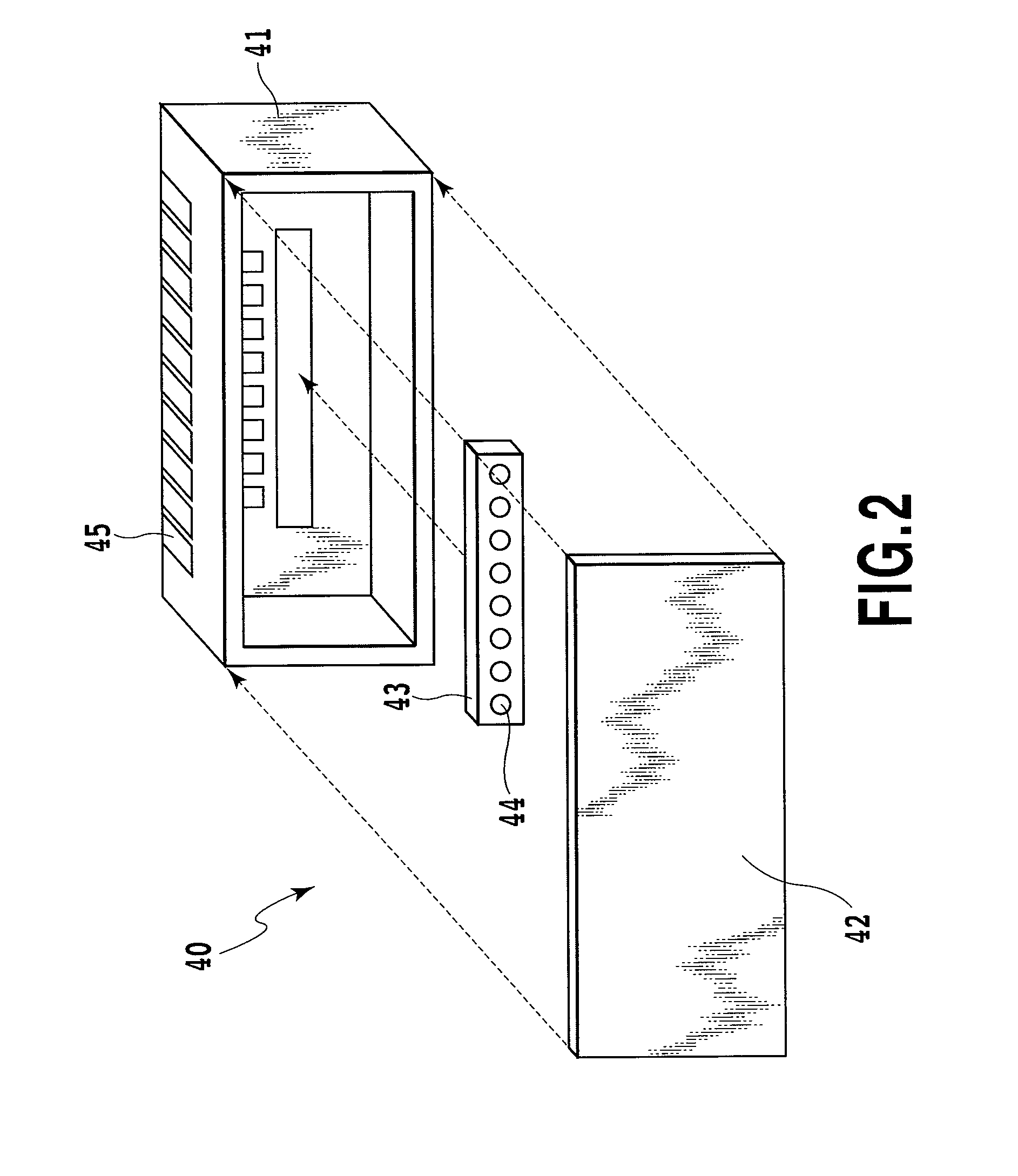
[0044]FIG. 4 illustrates a configuration of an optical module according to Embodiment 1 of the present invention. The optical module 1 is a 16-channel optical power monitor that has the PLC 30 having an AWG having 16 output waveguides 37. An end face of the PLC 30 is joined to the two PD packages 40a and 40b storing therein the 8-channel PD array 43. The optical module 1 is structured so that the printed circuit board 200 including the PLC 30, the PD packages 40a and 40b, and the connectors 22a and 22b is provided in the housing 3. A wavelength division multiplexing signal of 16 waves input from the optical fiber 2 is branched by the AWG to optical signals having individual wavelengths and the signals are received by the light-receiving faces of the individual PDs stored in the PD packages 40a and 40b.

[0045]FIG. 5 illustrates a method of fixing the PLC and the PD packages according to Embodiment 1. FIG. 5 is a cross-sectional view taken along V-V in FIG. 4. The output waveguide 37 ...

embodiment 2

[0048]FIG. 7 illustrates a configuration illustrating an optical module according to Embodiment 2 of the present invention. The optical module 1 is a 16-channel optical power monitor that has the PLC 30 having an AWG having 16 output waveguides 37. An end face of the PLC 30 is joined to the two PD packages 40a and 40b storing therein the 8-channel PD array 43. The optical module 1 is structured so that the printed circuit board 200 including the PLC 30, the PD packages 40a and 40b, and the connectors 22a and 22b is provided in the housing 3. A wavelength division multiplexing signal of 16 waves input from the optical fiber 2 is branched by the AWG to optical signals having individual wavelengths and the signals are received by the light-receiving faces of the individual PDs stored in the PD packages 40a and 40b.

[0049]A cross-sectional view taken along VIII-VIII of FIG. 7 is identical as that of FIG. 3. Embodiment 2 is different from the conventional optical module in the printed ci...

embodiment 3

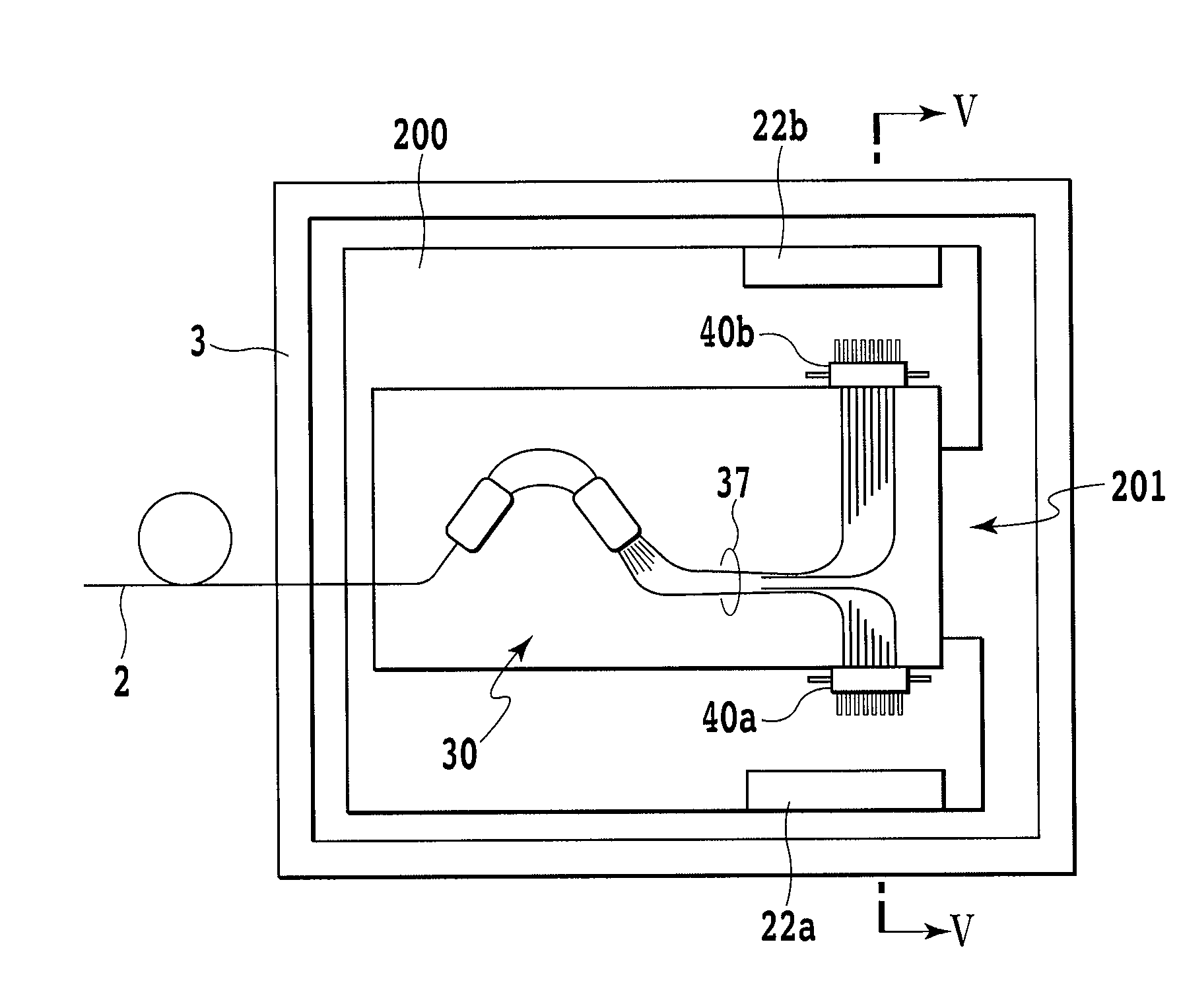
[0050]FIG. 8 illustrates the configuration of an optical module according to Embodiment 3 of the present invention. The optical module 1 is a 16-channel optical power monitor that has the PLC 30 having an AWG having 16 output waveguides 37. An end face of the PLC 30 is joined to the two PD packages 40a and 40b storing therein the 8-channel PD array 43. The optical module 1 is structured so that the printed circuit boards 220a and 220b respectively including the PLC 30, the PD packages 40a and 40b, and the connectors 22a and 22b are provided in the housing 3. A wavelength division multiplexing signal of 16 waves input from the optical fiber 2 is branched by the AWG to optical signals having individual wavelengths and the signals are received by the light-receiving faces of the individual PDs stored in the PD packages 40a and 40b.

[0051]A cross-sectional view taken along V-V of FIG. 8 is identical as that of FIG. 5. Embodiment 3 is different from Embodiment 1 in the printed circuit bo...


PUM


Abstract

An optical module has a structure for reducing the stress applied to a package. The optical module is structured so that an end face of a waveguide (37) of a planar lightwave circuit (30) is joined to a plurality of packages (40) storing therein optical elements so that the waveguide is optically coupled to the optical elements. The optical module includes a housing (3) storing therein a planar lightwave circuit and a plurality of packages in which an upper face of a protrusion (270) formed in the bottom section is fixed to the planar lightwave circuit (30). Each of the plurality of packages (40) is electrically connected to an electric part (22) provided in the housing (3) via flexible printed circuits (271a, 271b).

Description

TECHNICAL FIELD[0001]The present invention relates to an optical module. In particular, the present invention relates to the structure of the optical module that is stable against temperature fluctuation.BACKGROUND ART[0002]In recent years, with the diffusion of optical fiber transmission, various techniques have been required to realize optical signal processing functions. Furthermore, a technique has been also required to integrate a great number of optical elements with a high density. Among the techniques as described above, a planar lightwave circuit (hereinafter referred to as PLC) is known. The PLC is generally an optical circuit that is structured so that an optical waveguide composed of a core and a clad for propagating an optical signal and optical function elements are integrated on a silicon substrate or a quartz substrate. The PLC is superior in productivity and reliability and is also superior in integration and high function. Thus, the development for an optical modul...

Claims


Application Information

Patent Timeline
Patent Type & Authority Applications(United States)
IPC IPC(8): G02B6/36
CPCH01S5/02248H01S5/02284G02B6/12019G02B6/30G02B6/42H01L2224/48091G02B6/4201H01S5/02208H01L2924/00014G02B6/4267G02B6/4283G02B6/4268G02B6/4281H01S5/02325H01S5/02251
Inventor OHYAMA, TAKAHARUDOI, YOSHIYUKIOGAWA, IKUOKANEKO, AKIMASATAMURA, YASUAKISUZUKI, YUICHI
Owner NIPPON TELEGRAPH & TELEPHONE CORP
Why Eureka
Try Eureka