Non-planar embedded polysilicon resistor

a polysilicon resistor, non-planar technology, applied in the direction of diodes, semiconductor devices, electrical equipment, etc., can solve the problems of poor temperature coefficient, high process variability of metal resistors, and increasing problems such as polysilicon depletion

Inactive Publication Date: 2010-12-30
INTEL CORP
View PDF8 Cites 18 Cited by
  • Summary
  • Abstract
  • Description
  • Claims
  • Application Information

AI Technical Summary

Problems solved by technology

As dimensions of the MOSFET continued to be scaled down in recent technology nodes, polysilicon depletion became an increasingly severe problem.
However, gate electrodes are no longer formed from aluminum.
Unfortunately, metal resistors often suffer from high process variability and a poor temperature coefficient.
However, such a change causes many challenges in process integration.

Method used


Image

  • Non-planar embedded polysilicon resistor
  • Non-planar embedded polysilicon resistor
  • Non-planar embedded polysilicon resistor

Examples


Embodiment Construction

[0010]In the following description, numerous details, examples, and embodiments are set forth to provide a thorough understanding of the present invention. However, it will become clear and apparent to one of ordinary skill in the art that the invention is not limited to the details, examples, and embodiments set forth and that the invention may be practiced without some of the particular details, examples, and embodiments that are described. In other instances, one of ordinary skill in the art will further realize that certain details, examples, and embodiments that may be well-known have not been specifically described so as to avoid obscuring the present invention.

[0011]The present invention discloses a non-planar embedded polysilicon resistor and a method of fabricating the non-planar embedded polysilicon resistor.

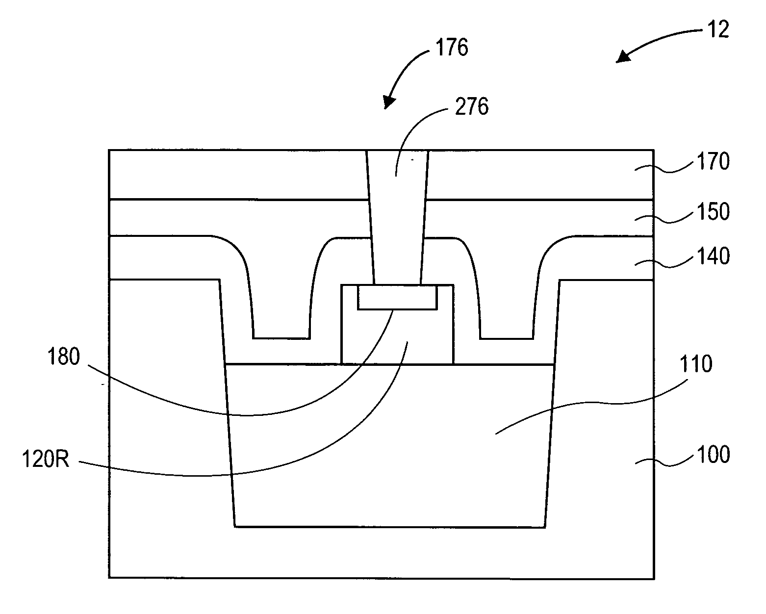
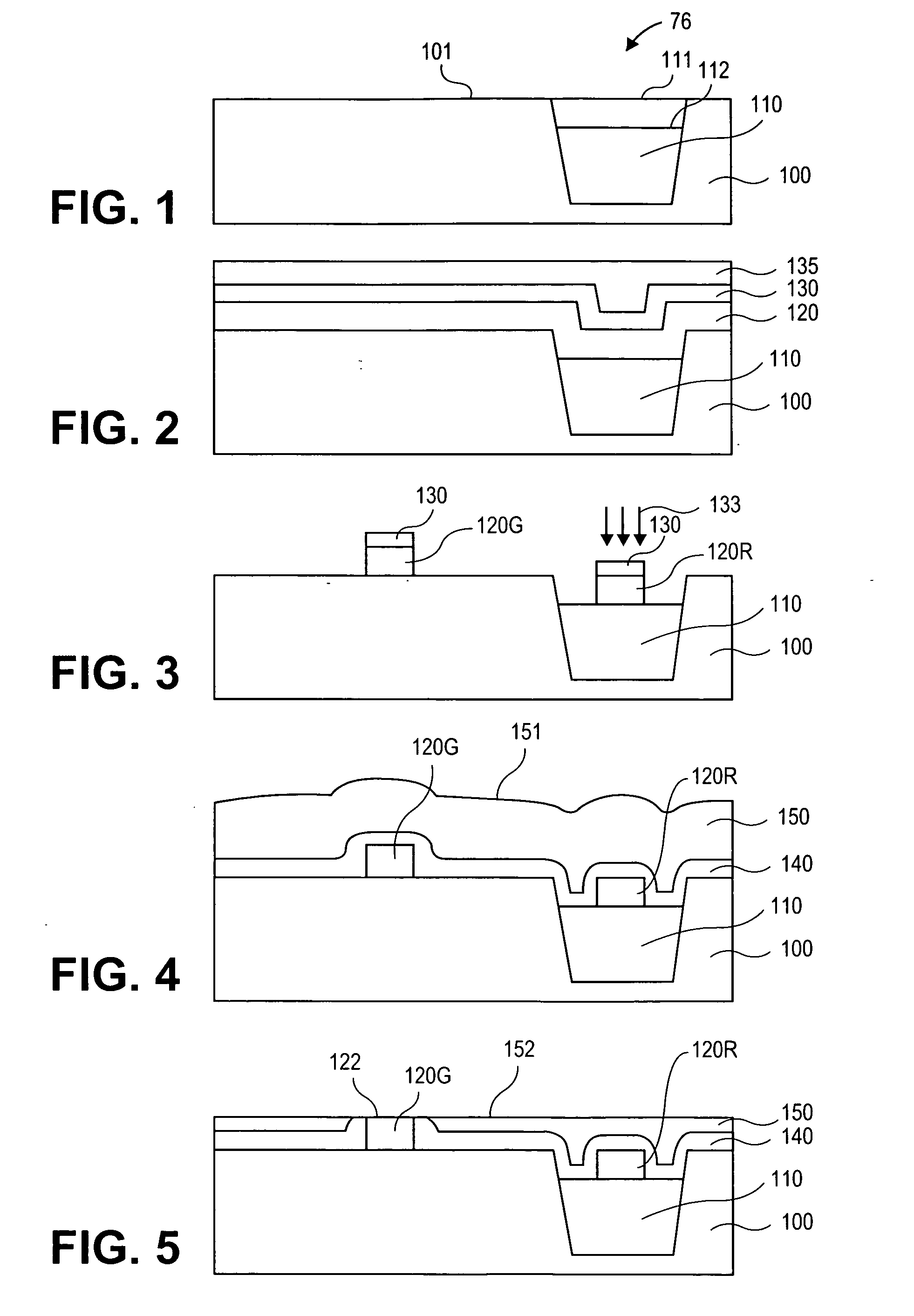
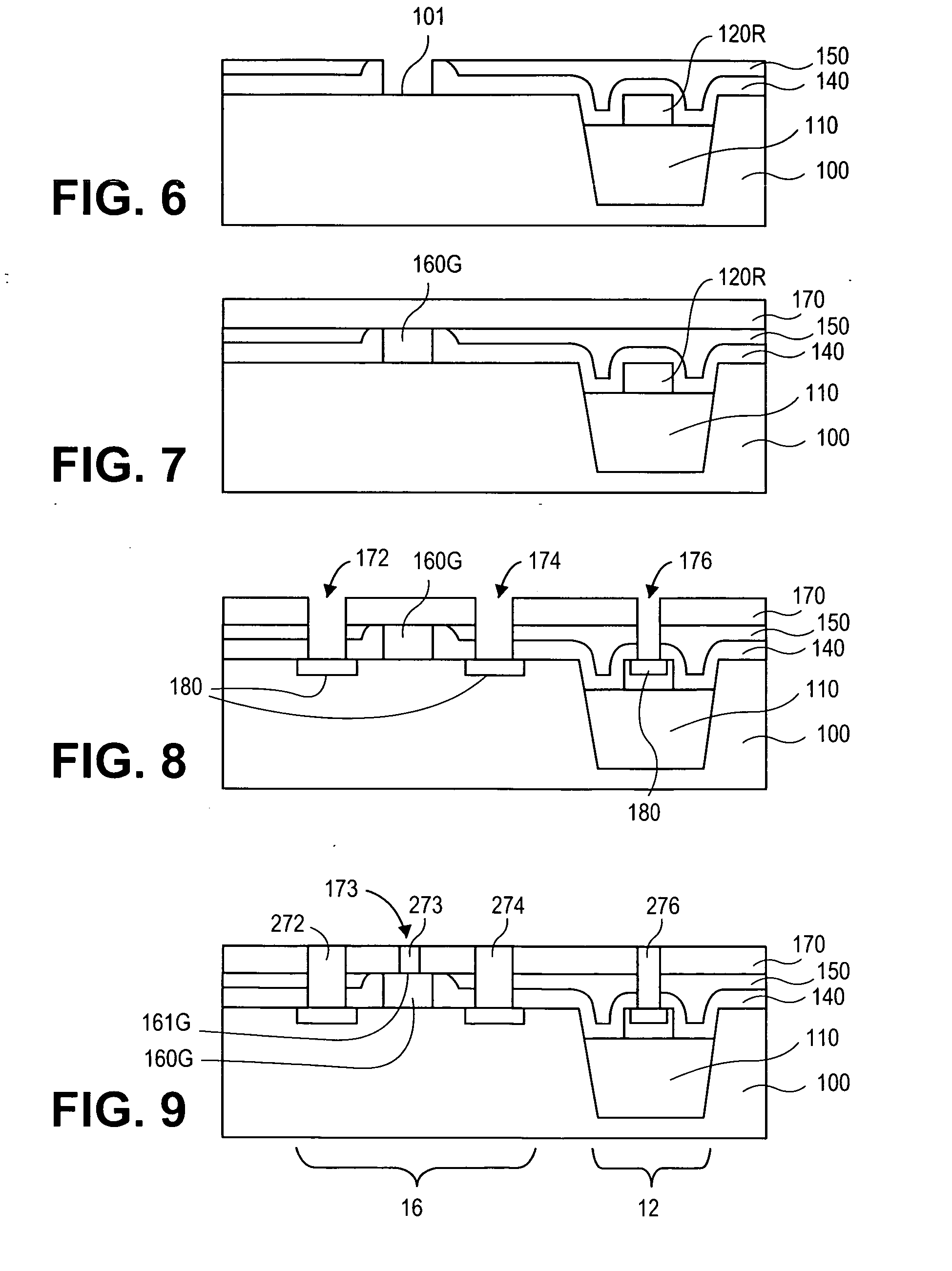
[0012]As shown in FIG. 1, a substrate 100 is provided that may comprise a bulk semiconductor, such as silicon, or a semiconductor-on-insulator (SOI).

[0013]An elongated...


PUM


Abstract

The present invention discloses a method comprising: forming a sacrificial polysilicon gate (of a transistor) and a polysilicon resistor; and replacing said sacrificial polysilicon gate (of said transistor) with a metal gate while covering said polysilicon resistor.

Description

BACKGROUND OF THE INVENTION[0001]1. Field of the Invention[0002]The present invention relates to a field of semiconductor devices, and, more specifically, to a high-precision resistor and a method of fabricating the high-precision resistor.[0003]2. Discussion of Related Art[0004]Gate electrodes were initially formed from metal (aluminum). However, for many technology nodes, a Metal-Oxide-Semiconductor Field Effect Transistor (MOSFET) had included a gate electrode that was fabricated from polysilicon so as to permit ion implantation (to customize doping to N- or P-type in the same circuit) and silicidation (to reduce contact resistance). Consequently, a resistor associated with the MOSFET in a circuit was also fabricated with polysilicon. A so-called “gate-first” process sequence was universally practiced so as to permit blanket deposition of the polysilicon, plasma etch-defined gate lengths, lightly-doped tip regions, dielectric sidewall spacers, and self-aligned source / drain (to th...

Claims


Application Information

Patent Timeline
Patent Type & Authority Applications(United States)
IPC IPC(8): H01L27/10H01L21/8234H01L21/02
CPCH01L21/28123H01L27/0629H01L29/78H01L29/4916H01L29/66545H01L28/20
Inventor JAN, CHIA-HONGYEH, JENG-YA
Owner INTEL CORP
Why Eureka
Try Eureka