Method of fabricating a semiconductor device having a nitride/high-k/nitride gate dielectric stack by atomic layer deposition (ALD) and a device thereby formed

a gate dielectric and high-k/nitride technology, applied in the direction of semiconductor devices, basic electric elements, electrical equipment, etc., can solve the problems of thermal instability, significant increase in direct tunneling leakage current through a very thin gate oxide, and the like, and achieve good thermal stability

Inactive Publication Date: 2005-03-15
ADVANCED MICRO DEVICES INC
View PDF9 Cites 49 Cited by
  • Summary
  • Abstract
  • Description
  • Claims
  • Application Information

AI Technical Summary

Benefits of technology

[0010]Accordingly, the present invention provides a method of fabricating a semiconductor device comprising a high-k dielectric gate insulator having good thermal stability which does not diffuse into a Si substrate, a poly-Si gate, or a poly-SiGe gate when experiencing subsequent high temperature processes, and a device thereby formed. Generally, the present invention device has a high-k gate dielectric insulator (i.e., a nitride / high-k material / nitride gate dielectric stack) formed by atomic layer deposition (ALD). The present invention method for fabricating the present device, generally comprises: depositing a first ultra-thin nitride film; depositing a high-k material film; and depositing a second ultra-thin nitride film. The unique features of the present method basically involve a sandwich structure formed by depositing an ultra-thin nitride film, which may comprise silicon nitride (Si3N4), before and after depositing the high-k material film, which may comprise a thin metal film, whereby the first ultra-thin nitride film provides resistance to metal diffusion into the Si substrate, the poly-Si gate electrode, or the poly-SiGe gate electrode. This present invention device, so formed, has the advantages of providing sufficient diffusion resistance as well as thermal stability in a thin (i.e., small) feature size.
[0012]Advantages of the present invention include the reduction of direct tunneling current flow through a gate dielectric insulator of a semiconductor device, and the fabrication of a semiconductor device comprising a high-k dielectric gate insulator having good thermal stability which does not diffuse into a Si substrate, a poly-Si gate, or a poly-SiGe gate when experiencing subsequent high temperature processes. Further advantages of the invention will be demonstrated in the following portions of the specification, wherein the detailed description is for the purpose of fully disclosing preferred embodiments of the invention without thereon placing limitations.

Problems solved by technology

In so doing, the related art has faced problems associated with a significant increase in direct tunneling leakage current through a very thin gate oxide (i.e., <25 Angstroms).
Another major problem with using a high-k material is thermal instability.

Method used


Image

  • Method of fabricating a semiconductor device having a nitride/high-k/nitride gate dielectric stack by atomic layer deposition (ALD) and a device thereby formed
  • Method of fabricating a semiconductor device having a nitride/high-k/nitride gate dielectric stack by atomic layer deposition (ALD) and a device thereby formed
  • Method of fabricating a semiconductor device having a nitride/high-k/nitride gate dielectric stack by atomic layer deposition (ALD) and a device thereby formed

Examples


Embodiment Construction

s.

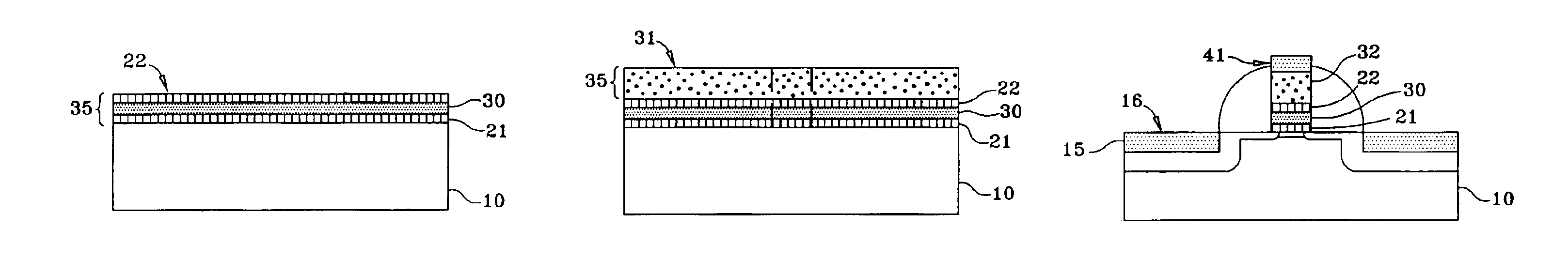
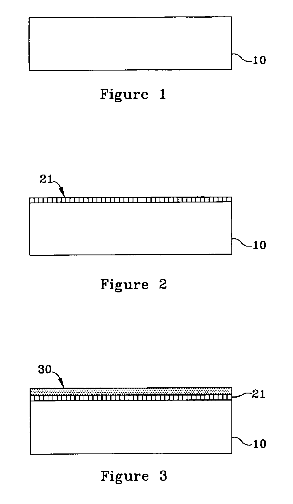
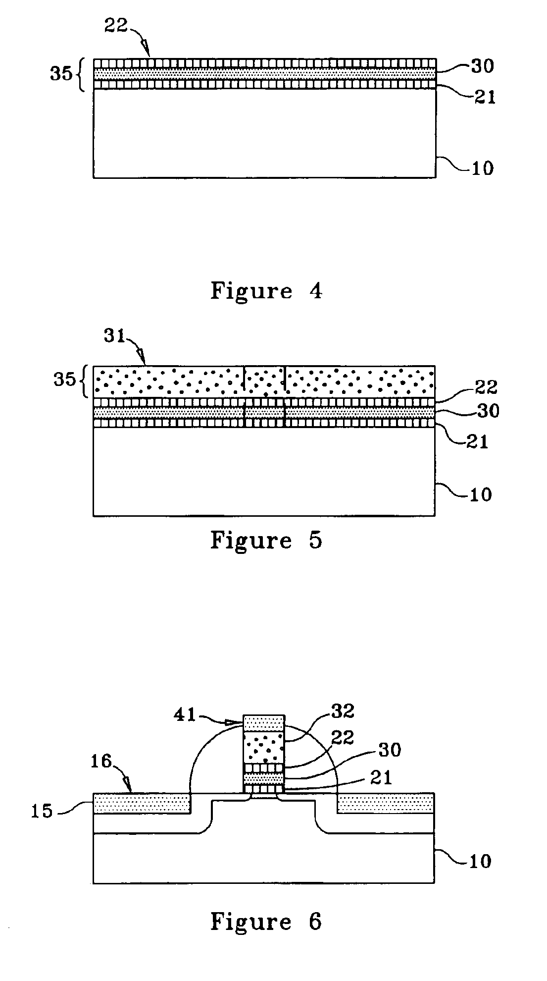
[0014]FIG. 1 through FIG. 6, together, constitute a process flow diagram of the fabrication of a semiconductor device, in accordance with the present invention, wherein the semiconductor device is shown in cross-section at various stages of the process.

DETAILED DESCRIPTION OF THE INVENTION

[0015]Referring more specifically to the drawings for illustrative purposes, the present invention is embodied in the apparatus and method generally shown in FIG. 1 through FIG. 6. These figures depict an embodiment of a process for fabricating a semiconductor device comprising a high-k dielectric gate insulator having good thermal stability which does not diffuse into a Si substrate, a poly-Si gate, or a poly-SiGe gate when experiencing subsequent high temperature processes. Each figure illustrates a particular processing stage, and presents a side view in cross-section of the device at that stage of processing. However, that the apparatus may vary as to configuration and as to details of the pa...


PUM

PropertyMeasurementUnit
thicknessaaaaaaaaaa
thermal stabilityaaaaaaaaaa
critical dimensionsaaaaaaaaaa

Abstract

A method of fabricating a semiconductor device, having a nitride / high-k material / nitride gate dielectric stack with good thermal stability which does not diffuse into a silicon substrate, a polysilicon gate, or a polysilicon-germanium gate when experiencing subsequent high temperature processes, involving: (a) providing a substrate; (b) initiating formation of the nitride / high-k material / nitride gate dielectric stack by depositing a first ultra-thin nitride film on the substrate; (c) depositing a high-k material, such as a thin metal film, on the first ultra-thin nitride film; (d) depositing a second ultra-thin nitride film on the high-k material, thereby forming a sandwich structure; (e) completing formation of the nitride / high-k material / nitride gate dielectric stack from the sandwich structure; and (f) completing fabrication of the semiconductor device.

Description

CROSS-REFERENCE TO RELATED APPLICATION(S)[0002]Not ApplicableSTATEMENT REGARDING FEDERALLY SPONSORED RESEARCH OR DEVELOPMENT[0003]Not ApplicableREFERENCE TO A MICROFICHE APPENDIX[0004]Not ApplicableBACKGROUND OF THE INVENTION[0005]1. Field of the Invention[0006]The present invention relates to semiconductor devices and their methods of fabrication. More particularly, the present invention relates to the formation of gate stacks. Even more particularly, the present invention relates to forming a gate stack having superior thermal stability and reduced diffusion into silicon-bearing semiconductor structures.[0007]2. Description of the Background Art[0008]Currently, the semiconductor industry has an interest in reducing the critical dimensions of transistors. As such, the thickness of the gate oxide must also be reduced. In so doing, the related art has faced problems associated with a significant increase in direct tunneling leakage current through a very thin gate oxide (i.e., <25...

Claims


Application Information

Patent Timeline
Patent Type & Authority Patents(United States)
IPC IPC(8): H01L21/02H01L21/28H01L29/51H01L21/318H01L21/314H01L29/40H01L29/49
CPCH01L21/28194H01L21/28202H01L21/3141H01L21/3144H01L29/518H01L29/513H01L29/517H01L21/3185H01L29/4908H01L21/0228H01L21/02186H01L21/0217H01L21/02189H01L21/022H01L21/02181
Inventor YU, BIN
Owner ADVANCED MICRO DEVICES INC
Why Eureka
Try Eureka