Strained silicon carbon alloy MOSFET structure and fabrication method thereof

a technology of strained silicon carbon alloy and mosfet, which is applied in the direction of semiconductor devices, electrical devices, transistors, etc., can solve the problems of ge content, asymmetrical speed increase between pmos and nmos, and drawback of asymmetrical speed increase, so as to improve device current driving force, reduce device dimensions, and increase strain quantity

Active Publication Date: 2005-02-03
TRANSPACIFIC IP LTD
View PDF5 Cites 51 Cited by
  • Summary
  • Abstract
  • Description
  • Claims
  • Application Information

AI Technical Summary

Benefits of technology

[0005] Accordingly, the main object of the present invention is to provide a transistor structure combining the merits of strained silicon formed on the relaxed buffer layer and a st

Problems solved by technology

The present technology, however, has the drawback of asymmetrical sp

Method used


Image

  • Strained silicon carbon alloy MOSFET structure and fabrication method thereof
  • Strained silicon carbon alloy MOSFET structure and fabrication method thereof
  • Strained silicon carbon alloy MOSFET structure and fabrication method thereof

Examples


Embodiment Construction

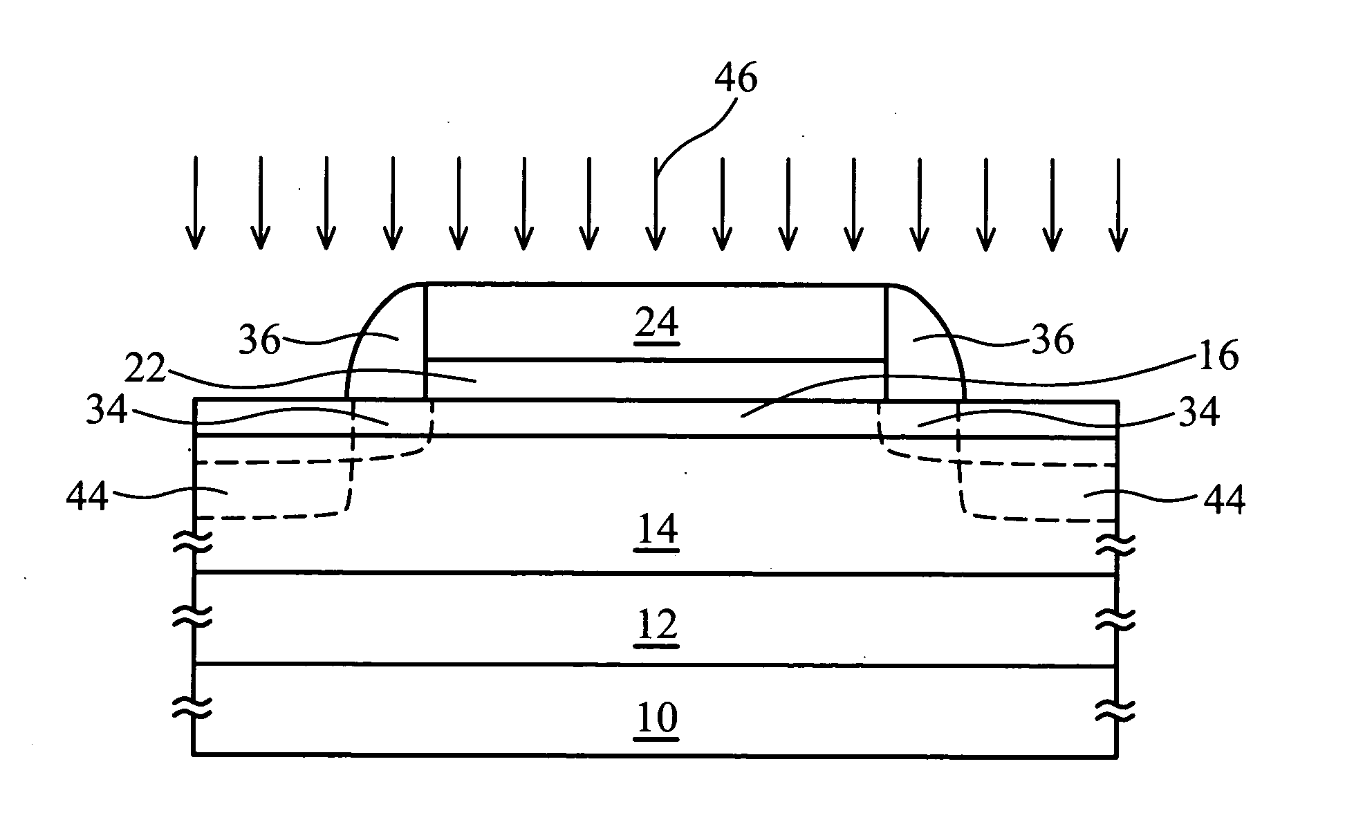
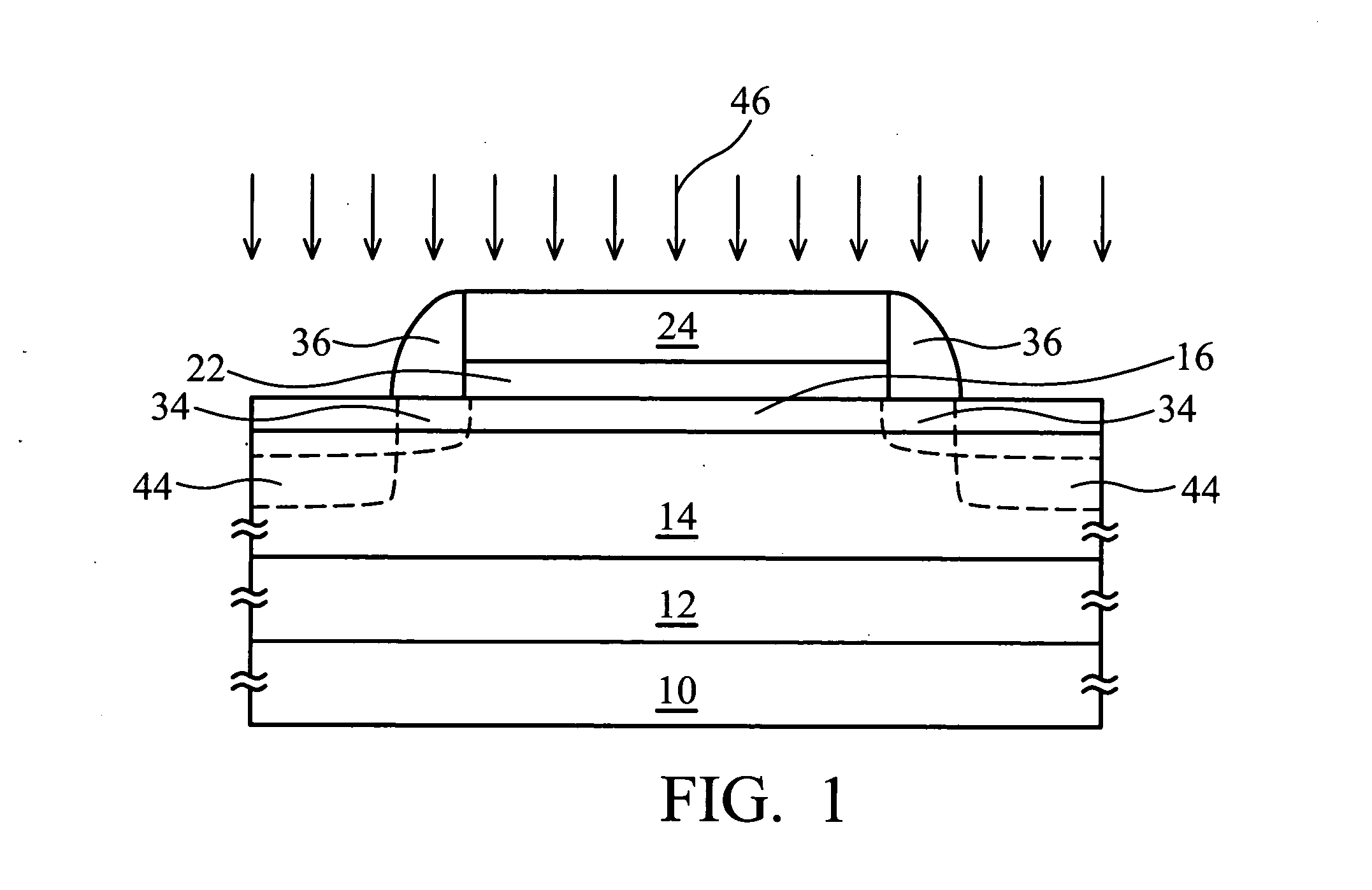
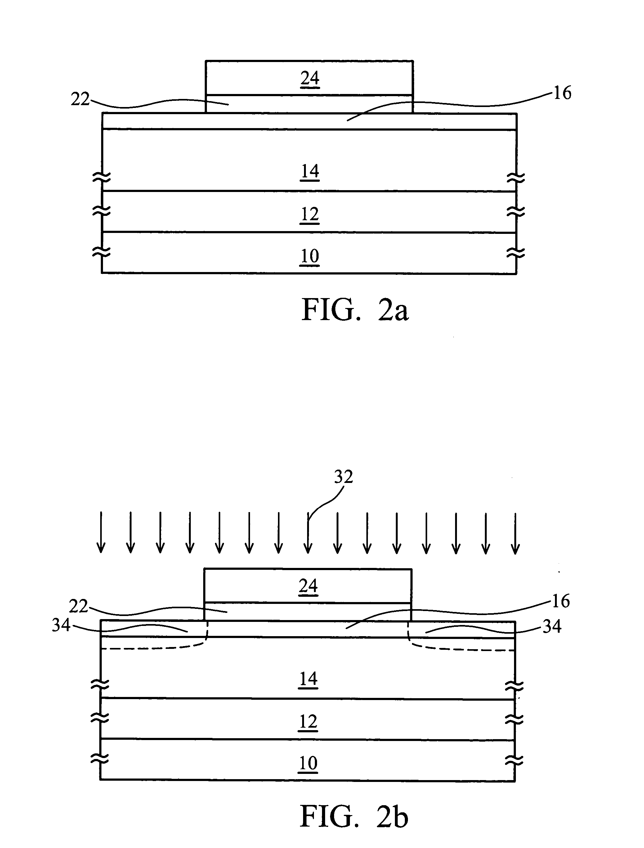
[0017] In this specification, “overlying the substrate”, “above the layer”, or “on the film” denote a relative positional relationship with respect to the surface of the base layer, regardless of the existence of intermediate layers. Accordingly, these expressions may indicate not only the direct contact of layers, but also, a non-contact state between one or more laminated layers. In addition, Silicon carbon alloy refers silicon carbon alloy, not silicon carbide.

[0018] According to the present invention, in FIG. 1, a strained silicon carbon alloy MOSFET structure comprises a substrate 10, such as a silicon substrate, a graded SiGe layer 12, a relaxed buffer layer 14, such as a relaxed SiGe buffer layer, a strained silicon carbon alloy layer 16, a gate dielectric layer 22, a ploysilicon gate electrode 24, a sidewall spacer 36, a source / drain extension region 34, and a source / drain region 44.

[0019] In FIG. 1, with a difference between Si and C in lattice constant of about 52%, the ...


PUM


Abstract

A MOSFET structure utilizing strained silicon carbon alloy and fabrication method thereof. The MOSFET structure includes a substrate, a graded SiGe layer, a relaxed buffer layer, a strained silicon carbon alloy channel layer, a gate dielectric layer, a polysilicon gate electrode (or metal gate electrode) and a source/drain region.

Description

BACKGROUND OF THE INVENTION [0001] 1. Field of the Invention [0002] The present invention relates in general to a structure of MOSFET. In particular, the present invention relates to a strained silicon carbon alloy MOSFET structure and fabrication method thereof. [0003] 2. Description of the Related Art [0004] In the present technology for fabricating metal-oxide-semiconductor field-effect transistor (MOSFET), strained silicon is formed on the relaxed SiGe layer to generate tensile strain. It had been confirmed that hole and electron mobility thereof are improved. Intel Corporation has implemented strained silicon technology into 90 nm process technology. The present technology, however, has the drawback of asymmetrical speed increasing between PMOS and NMOS even under the same Ge content. Theoretically, when using carbon doping to increase strain of the strained silicon channel, a highly increased current driving force and device speed of PMOS, and therefore improved symmetry of th...

Claims


Application Information

Patent Timeline
IPC IPC(8): H01L21/336H01L29/10
CPCH01L29/1054H01L29/6659
Inventor LEE, MIN-HUNGCHANG, SHULU, SHINGLIU, CHEE-WEE
Owner TRANSPACIFIC IP LTD
Why Eureka
Try Eureka