Gate electrode forming methods using conductive hard mask

a gate electrode and hard mask technology, applied in the direction of semiconductor devices, basic electric elements, electrical equipment, etc., can solve the problems of gate leakage current becoming unacceptably high, reducing the capacitance of the gate, and affecting the device performance, so as to prevent the process from damage

Inactive Publication Date: 2006-03-30
IBM CORP
View PDF19 Cites 48 Cited by
  • Summary
  • Abstract
  • Description
  • Claims
  • Application Information

AI Technical Summary

Benefits of technology

[0010] The invention includes methods related to formation of a gate electrode that employ a conductive hard mask as a protective layer during a photoresist removal process. In preferred embodiments, the conductive hard mask includes a metal containing conductor or a metal silicide. The invention prevents process damage on the gate dielectric during wet and / or dry resist strip, and since the conductive hard mask cannot be etched in typical resist strip chemistries, the invention also protects a metal electrode under the hard mask. The steps disclosed allow creation of a multiple work function metal gate electrode, or a mixed metal and polysilicon gate electrode, which do not suffer from the problems of the related art.

Problems solved by technology

The ongoing reduction in size of electronic device elements poses problems in device performance that must be addressed using new materials and fabrication techniques.
If a conventional oxynitride gate dielectric is used, decreasing the thickness below about 1.2 nm (physical thickness of the dielectric) causes the gate leakage current to become unacceptably high.
The appearance of this depletion region reduces the capacitance of the gate and thus increases the electrical thickness.
If a gate structure about this size is designed with a gate dielectric equivalent thickness of about 1 nm, a conventional oxynitride gate dielectric can no longer be used due to unacceptably high leakage currents.
However, the combination of polysilicon for gate conductor 18 with a high-k material for gate dielectric 20 presents further problems.
In particular, an increased Vt may prevent proper function in a PFET.
Another problem affecting PFET performance is that of penetration of boron from the p+ type polysilicon into the high-k dielectric and possibly into the channel region of the device, which renders the device unusable.
In addition, the boron diffusion also interferes with hafnium containing high-k dielectrics.
Unfortunately, current technology implements such a photoresist strip with the aid of an oxidizing ambient (e.g. oxygen or ozone plasma) and / or an oxidizing chemical solution (e.g. a solution of sulfuric acid (H2SO4) with oxidizing peroxide H2O2).
Presence of oxidizers (dry or wet) can substantially thicken the exposed gate dielectric which leads to a substantial degradation of performance.
The absence of oxidizing agents in the resist strip can lead to a defective layer formation in the gate dielectric and the gate electrode.
For example, the non-oxidizing solvent resist strip can create impurity contamination like carbon on a gate oxide and incomplete uniform resist strip.
Accordingly, the first gate material can be also damaged during a typical photoresist strip process.

Method used


Image

  • Gate electrode forming methods using conductive hard mask
  • Gate electrode forming methods using conductive hard mask
  • Gate electrode forming methods using conductive hard mask

Examples


Embodiment Construction

[0019] With reference to the accompanying drawings, the invention will be described in terms of a method for creating a metal gate electrode with multiple work functions. It should be recognized, however, that other inventive methods are included within this method, as denoted by the appended claims.

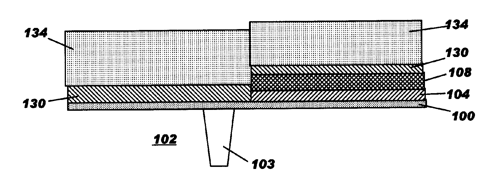
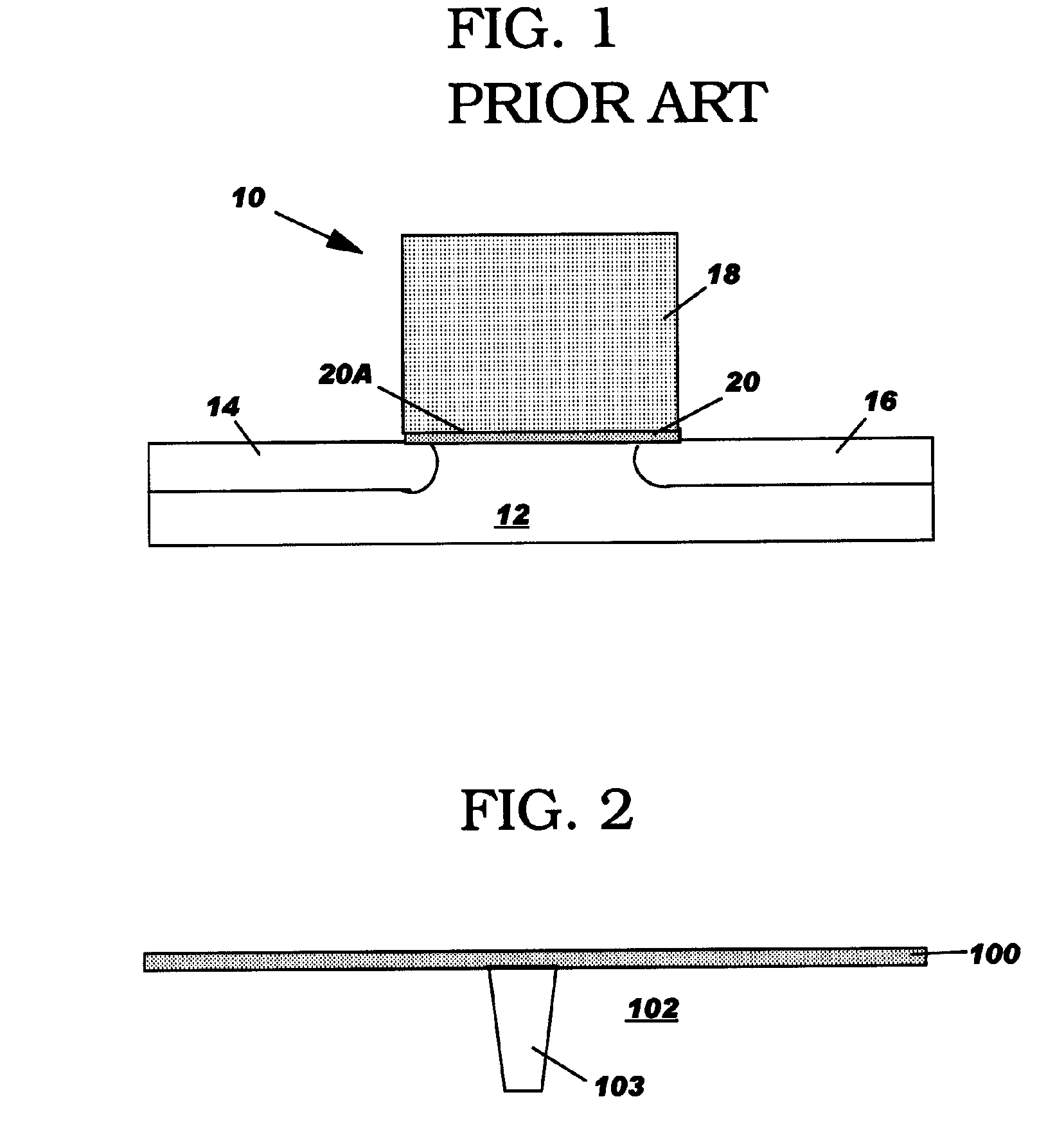
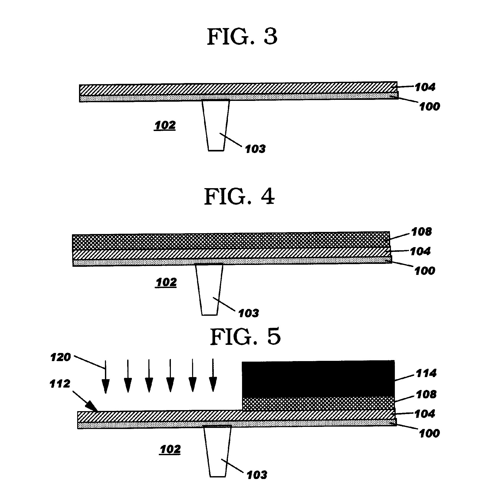
[0020] Referring to FIG. 2, in a first step of the method, a dielectric 100 is formed upon a substrate 102, which may include shallow trench isolation (STI) 103. Substrate 102 can also include other useful structures which are not essential to the instant invention and not shown for clarity. Such useful structures may include but are not limited to: buried dielectric layers and buried interconnects, memory cells, trench capacitors, and stress inducing layers and structures. Dielectric 100 may be deposited in any now known or later developed fashion such as by a combination of thermal nitridation and oxidation, or an atomic layer deposition (ALD). Dielectric 100 may include any conventio...


PUM

PropertyMeasurementUnit
thicknessaaaaaaaaaa
physical thicknessaaaaaaaaaa
thicknessaaaaaaaaaa

Abstract

Methods related to formation of a gate electrode are disclosed that employ a conductive hard mask as a protective layer during a photoresist removal process. In preferred embodiments, the conductive hard mask includes a metal containing conductor or a metal silicide. The invention prevents process damage on the gate dielectric during wet and/or dry resist strip, and since the conductive hard mask cannot be etched in typical resist strip chemistries, the invention also protects a metal electrode under the hard mask. The steps disclosed allow creation of a multiple work function metal gate electrode, or a mixed metal and polysilicon gate electrode, which do not suffer from the problems of the related art.

Description

BACKGROUND OF INVENTION [0001] 1. Technical Field [0002] This invention relates to the manufacture of advanced semiconductor devices, and more particularly, to a method related to formation of a gate electrode that employs a conductive hard mask as a protective layer during a photoresist removal process for multiple work function gate structures. [0003] 2. Related Art [0004] The ongoing reduction in size of electronic device elements poses problems in device performance that must be addressed using new materials and fabrication techniques. In the case of gate structures for high-performance complementary metal-oxide semiconductor (CMOS) devices, the equivalent oxide thickness of the gate dielectric has been reduced to about 1.2 nm. A typical CMOS gate structure is shown schematically in FIG. 1. Gate structure 10 is fabricated on the surface of a substrate 12, which has source and drain regions 14, 16 formed therein. Gate structure 10 includes conducting element 18 (typically polysil...

Claims


Application Information

Patent Timeline
Patent Type & Authority Applications(United States)
IPC IPC(8): H01L21/3205
CPCH01L21/28079H01L21/32139H01L29/518H01L29/4958H01L29/517H01L21/823842
Inventor GLUSCHENKOV, OLEGPARK, DAE-GYU
Owner IBM CORP
Why Eureka
Try Eureka