Package process and package structure

a technology of packaging and process, applied in the direction of printed circuit, sustainable manufacturing/processing, final product manufacturing, etc., can solve the problems of reducing the production yield rate, and achieve the effect of reducing the thickness of the packag

Inactive Publication Date: 2010-12-30
ADVANCED SEMICON ENG INC
View PDF11 Cites 54 Cited by
  • Summary
  • Abstract
  • Description
  • Claims
  • Application Information

AI Technical Summary

Benefits of technology

[0007]The present invention is directed to a package structure having a thinner semiconductor substrate for reducing a thickness of the package.
[0032]In light of the foregoing, since the thickness of the semiconductor substrate in the present invention is thinner (i.e. under 8 mils), when the chip is bonded on the semiconductor substrate by the flip chip technique and encapsulated by the molding compound to form the package structure, this package structure has a thinner package thickness. In addition, as the semiconductor substrate of the present invention is supported by the carrier, the fracture of semiconductor substrate during the flip chip bonding of the chip onto the semiconductor substrate is prevented. Furthermore, since the semiconductor substrate is first packaged by the molding compound and then cut, the strength of the semiconductor substrate is relatively enhanced to prevent the fracture of the semiconductor substrate so as to lower the difficulty in the subsequent process and facilitate in enhancing the production yield rate. Moreover, it is suitable for mass production.

Problems solved by technology

Since the process capacitance of bonding the chip to the wafer by using the flip chip bonding technique still has its limit value, when the thickness of the wafer used is smaller than the limit value of the process capacitance thereof, fracture often results in the flip chip bonding process, thereby reducing the production yield rate.

Method used


Image

  • Package process and package structure
  • Package process and package structure
  • Package process and package structure

Examples


Embodiment Construction

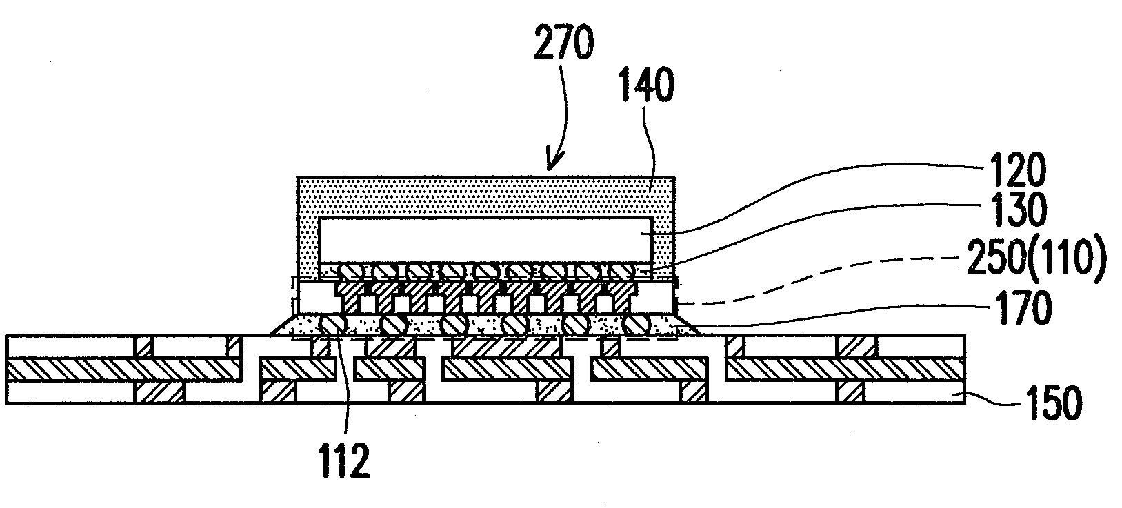
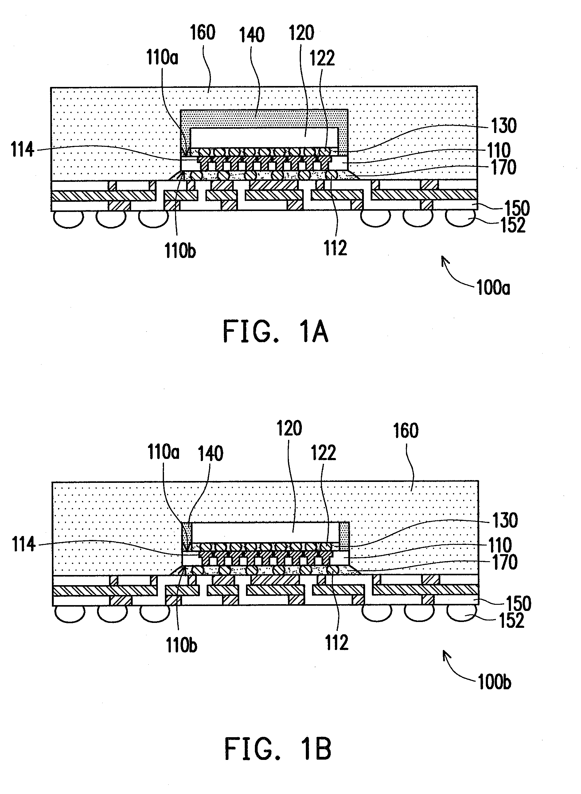
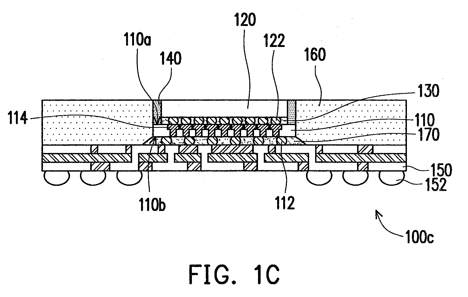
[0044]FIG. 1A is a schematic cross-sectional view of a package structure according to an embodiment of the present invention. Referring to FIG. 1A, a package structure 100a includes a semiconductor substrate 110, a chip 120, a first underfill 130, and a first molding compound 140.

[0045]The semiconductor substrate 110 is, for example, a silicon substrate and has an upper surface 110a. Here, a thickness of the semiconductor substrate 110 is under 8 mils, such as under 4 mils or even 2 mils. The chip 120 is disposed on the upper surface 110a of the semiconductor substrate 110 and a bottom of the chip 120 has a plurality of first conductive bumps 122. The first underfill 130 is disposed between the semiconductor substrate 110 and the chip 120 to encapsulate the first conductive bumps 122. The first molding compound 140 is disposed on the semiconductor substrate 110 and encapsulates a side surface of the chip 120, the first underfill 130, and a top surface of the chip 120. A side of the ...


PUM


Abstract

A package process is provided. First, a semiconductor substrate is disposed on a carrier, in which a surface of the carrier has an adhesive layer and the semiconductor substrate is bonded to the carrier by the adhesive layer. Next, a chip is bonded on the semiconductor substrate by flip chip technique and a first underfill is formed between the chip and the semiconductor substrate to encapsulate a plurality of first conductive bumps at the bottom of the chip. Then, a first molding compound is formed on the semiconductor substrate. The first molding compound at least encapsulates the side surface of the chip and the first underfill. Finally, the semiconductor substrate together with the chip and the first molding compound located thereon are separated from the adhesive layer of the carrier to form an array package structure.

Description

CROSS-REFERENCE TO RELATED APPLICATION[0001]This application claims the priority benefit of Taiwan application serial no. 98121414, filed on Jun. 25, 2009. The entirety of the above-mentioned patent application is hereby incorporated by reference herein and made a part of this specification.BACKGROUND OF THE INVENTION[0002]1. Field of the Invention[0003]The present invention relates to a semiconductor process and a structure thereof, and more particularly, to a package process and a package structure thereof.[0004]2. Description of Related Art[0005]With recent advancement of semiconductors and packaging techniques, the fabrication of micro devices including micro-electromechanical devices or electro-optical devices is currently achieved by adopting a prevailing wafer packaging technique rather than a chip packaging technique. Thereby, packaging costs are reduced, and the requirements for lightweight, slimness, compactness, and small volume are satisfied. In details, the wafer level ...

Claims


Application Information

Patent Timeline
Patent Type & Authority Applications(United States)
IPC IPC(8): H01L23/31H01L21/60
CPCH01L21/563H01L2224/16235H01L23/147H01L23/3128H01L23/3135H01L23/49822H01L23/49827H01L23/49833H01L24/16H01L24/81H01L24/97H01L2221/68345H01L2224/16H01L2224/48091H01L2224/73203H01L2224/75252H01L2224/83192H01L2224/97H01L2924/15311H01L2924/18161H01L2924/30105H05K3/007H05K3/284H05K3/3436H05K3/3478H05K2201/10674H05K2203/041H05K2203/1316H01L21/6835H01L2224/81005H01L2924/014H01L24/48H01L2924/00014H01L2224/81H01L2224/16225H01L2224/32225H01L2224/83005H01L2924/00011H01L2924/157H01L2924/181Y02P70/50H01L2224/83H01L2924/00012H01L2224/0401H01L2224/45099H01L2224/45015H01L2924/207
Inventor SHEN, CHI-CHIHCHEN, JEN-CHUANPAN, TOMMY
Owner ADVANCED SEMICON ENG INC
Why Eureka
Try Eureka