Supplying Power to Integrated Circuits Using a Grid Matrix Formed of Through-Silicon Vias

a grid matrix and silicon via technology, applied in the direction of electrical equipment, semiconductor devices, semiconductor/solid-state device details, etc., can solve the problems of significant amount of routing resource taken by the power mesh, high power dissipation, and increased design complexity, so as to reduce the use of chip area, reduce the blockage of signal routing, and reduce the effect of ir drop

Active Publication Date: 2011-01-06
TAIWAN SEMICON MFG CO LTD
View PDF12 Cites 38 Cited by
  • Summary
  • Abstract
  • Description
  • Claims
  • Application Information

AI Technical Summary

Benefits of technology

[0008]The advantageous features of the present invention include reduced chip area usage, reduced blockage to signal routing due to the power routing, and reduced IR drop.

Problems solved by technology

With advanced technologies for forming circuits having small sizes, the design complexity is increased dramatically, which leads to a high power dissipation.
In addition, a significant amount of routing resource is taken by the power mesh.
This results in a significant increase in the chip size as well as production cost.
An additional problem of the conventional power supply scheme as shown in FIGS. 1 and 2 is that stacked metal lines 22 and vias 24 occupy the chip area that otherwise would be used for routing, and hence they block the routing of signals and result in congestion.

Method used


Image

  • Supplying Power to Integrated Circuits Using a Grid Matrix Formed of Through-Silicon Vias
  • Supplying Power to Integrated Circuits Using a Grid Matrix Formed of Through-Silicon Vias
  • Supplying Power to Integrated Circuits Using a Grid Matrix Formed of Through-Silicon Vias

Examples


Embodiment Construction

[0023]The making and using of the embodiments of the present invention are discussed in detail below. It should be appreciated, however, that the embodiments provide many applicable inventive concepts that can be embodied in a wide variety of specific contexts. The specific embodiments discussed are merely illustrative of specific ways to make and use the invention and do not limit the scope of the invention.

[0024]A novel power distribution network, which includes a power grid for supplying power to integrated circuits and the method of designing the same are presented. The variations of the embodiment are discussed. Throughout the various views and illustrative embodiments of the present invention, like reference numbers are used to designate like elements.

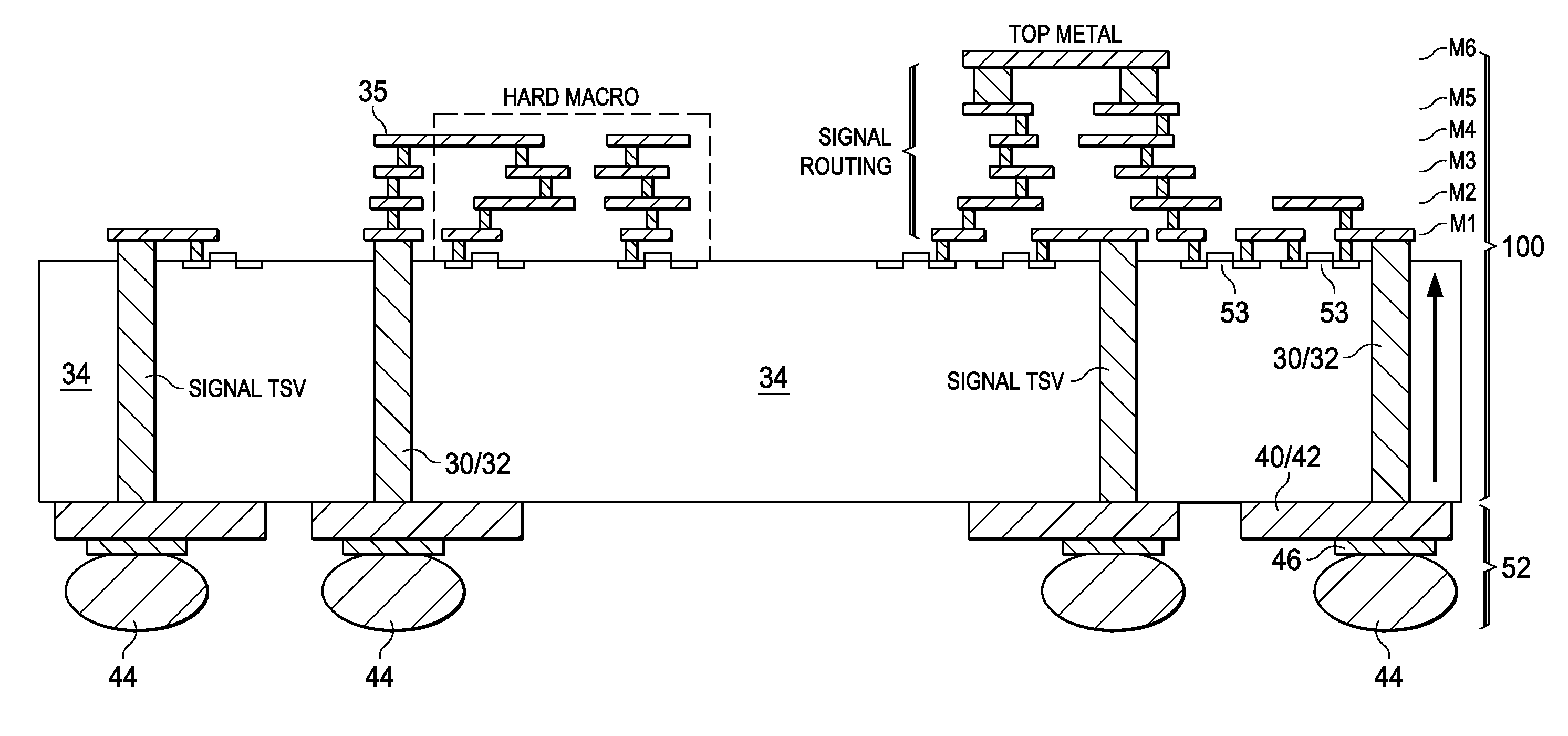
[0025]FIG. 3A illustrates a backside view of chip 100, wherein the backside is the side having no active devices, such as transistors formed thereon. The backside is on an opposite side of chip 100 than a front side, at which int...


PUM


Abstract

An integrated circuit structure includes a chip including a substrate and a power distribution network. The power distribution network includes a plurality of power through-silicon vias (TSVs) penetrating the substrate, wherein the plurality of power TSVs forms a grid; and a plurality of metal lines in a bottom metallization layer (M1), wherein the plurality of metal lines couples the plurality of power TSVs to integrated circuit devices on the substrate.

Description

[0001]This application claims the benefit of U.S. Provisional Application No. 61 / 223,315 filed on Jul. 7, 2009, entitled “Supplying Power to Integrated Circuits Using a Grid Matrix Formed of Through-Silicon Vias,” which application is hereby incorporated herein by reference.TECHNICAL FIELD[0002]This invention relates generally to integrated circuit structures, and more particularly to structures for supplying power to integrated circuits.BACKGROUND[0003]For the operation of integrated circuits, power must be supplied and distributed appropriately. This requires the appropriate distribution of operation voltages VDD and VSS. FIG. 1, which is a top view of a semiconductor chip, illustrates a power distribution scheme for distributing operation voltages VDD and VSS throughout a chip. VDD lines 10, which form a mesh, are distributed throughout the respective chip and carry operation voltage VDD. VSS lines 14, which also form a mesh, are distributed throughout the respective chip and car...

Claims


Application Information

Patent Timeline
Patent Type & Authority Applications(United States)
IPC IPC(8): H01L23/52
CPCH01L23/481H01L23/5286H01L2224/02372H01L2224/13023H01L2224/05008H01L2224/05025H01L2224/0401
Inventor LAW, OSCAR M. K.WU, KUO H.YEH, WEI-CHIH
Owner TAIWAN SEMICON MFG CO LTD
Why Eureka
Try Eureka