Thin-film solar cell module

a solar cell module and thin film technology, applied in the direction of photovoltaics, electrical devices, semiconductor devices, etc., can solve the problems of large integration loss, difficult to increase the number of integration stages, and relatively small substrate size of thin film solar cell modules, etc., to achieve high voltage output and maintain hotspot resistance

Inactive Publication Date: 2011-01-13
SHARP KK
View PDF3 Cites 40 Cited by
  • Summary
  • Abstract
  • Description
  • Claims
  • Application Information

AI Technical Summary

Benefits of technology

[0017]According to the thin-film solar cell module of the present invention, it is possible to achieve a thin-film solar cell module of high voltage output, while maintaining hotspot resistance.

Problems solved by technology

However, the size of substrates of thin-film solar cell modules has been relatively small so far, and integration loss grows too big if the number of integrated cells is increased aggressively.
Therefore, it has been difficult to increase the number of integration stages.
In addition, there have not been so many applications that require a high voltage of 200 V or more.
Therefore, there have not been produced so many thin-film solar cell modules that output a high voltage of 200 V or more.

Method used


Image

  • Thin-film solar cell module
  • Thin-film solar cell module
  • Thin-film solar cell module

Examples


embodiment 1

Embodiment of 53 Stages×12 Parallels×2 Blocks in Series

[0087]FIG. 5 illustrates an integrated thin-film solar cell module according to Embodiment 1 of the present invention, and FIG. 5 (a) is a plan view, FIG. 5 (b) is a cross-sectional view taken along lines A-B of FIG. 5 (a), and FIG. 5 (c) is a cross-sectional view taken along lines C-D of FIG. 5 (a). FIG. 6 illustrates a circuit diagram.

[0088]In Embodiment 1, a supporting substrate 1 is, for example, a translucent glass substrate or a resin substrate such as a polyimide. On the substrate (surface), a first electrode (for example, a transparent conductive film of SnO2 (tin oxide)) is formed by a thermal CVD method or the like. As long as the first electrode is a transparent electrode, it may be, for example, ITO which is a mixture of SnO2 and In2O3. Thereafter, the transparent conductive film is appropriately removed by patterning to form dividing scribe lines 3. Formation of the dividing scribe lines 3 forms the first electrode ...

embodiment 2

Embodiment of 53 Stages×6 Parallels×4 Blocks in Series

[0123]FIG. 7 illustrates an integrated thin-film solar cell module according to Embodiment 2 of the present invention, and FIG. 7(a) is a plan view, FIG. 7(b) is a cross-sectional view taken along lines E-F of FIG. 7(a), and FIG. 7(c) is a cross-sectional view taken along lines G-H of FIG. 7(a). FIG. 8 illustrates a circuit diagram.

[0124]Embodiment 2 is characterized in a connection method after division in order to output a higher voltage. The other configurations and the production method are the same as those of Embodiment 1. Specifically, processes up to the formation of the first electrode 2, the dividing scribe lines 3, the photoelectric conversion film 4, the second electrode 5, and the cell dividing grooves 6 are the same as those of Embodiment 1. Successively, the cell string is divided to 12 unit cell strings by the cell string dividing grooves 8 running in the vertical direction. At the time of the division, a middle s...

embodiment 3

Embodiment of 48 Stages×5 Parallels×4 Blocks in Series Achieved by Using Two Substrates of 48 Stages×5 Parallels×2 Blocks in Series

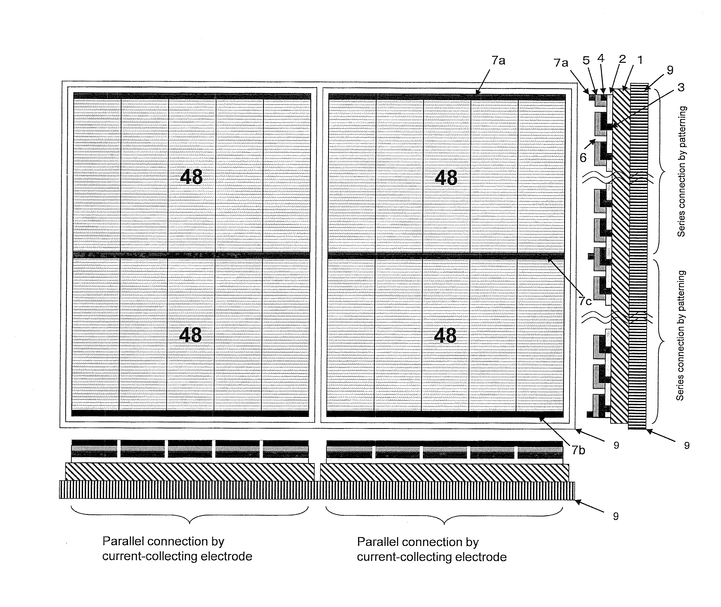
[0129]As for Embodiments 1 and 2, the supporting substrate itself is large, and have been described examples of the thin-film solar cell module in which all cell strings are formed on the substrate. However, even in the case where a plurality of small supporting substrates are combined to form a large solar cell module, similar problems will arise. In that case, a module of high voltage can be produced while ensuring reliability by forming cell strings in respective supporting substrates so that the requirement shown in the formula (1) is met and connecting the cell strings together. That is, the cell strings are formed in the same manner as in Embodiments 1 and 2, and arranged in two small sized integrated substrates connected in parallel on one integrated substrate 9 as illustrated in FIG. 9. That is, two supporting substrates 1 of the thin-film solar ...


PUM


Abstract

To provide an integrated thin-film solar cell that prevents deterioration of hotspot resistance and has a high output voltage.A thin-film solar cell module comprising: a thin-film solar cell string comprising a plurality of thin-film solar cell elements interconnected in series, each of the thin-film solar cell elements including a surface electrode, a photoelectric conversion layer, and a back surface electrode laminated in this order, the thin-film solar cell module being configured so that the number of stages n of the series connection of the thin-film solar cell elements in the thin-film solar cell string satisfies the following formula (1):n<Rshm / 2.5 / Vpm×Ipm+1  (1),wherein Rshm is the most frequent short-circuit resistance value of the thin-film solar cell elements;Vpm is an optimum operation voltage of the thin-film solar cell elements; andIpm is an optimum operation current of the thin-film solar cell elements.

Description

TECHNICAL FIELD[0001]The present invention relates to a thin-film solar cell module comprising a thin-film solar cell string comprising a plurality of thin-film solar cell elements connected in series. In particular, the thin-film solar cell module of the present invention is adapted to have high hotspot resistance.BACKGROUND ART[0002]A measure for increasing an output voltage of a solar cell module by connecting solar cells in series is well known. In particular, thin-film solar cell modules based on silicons including amorphous silicons, microcrystalline silicons, and polycrystalline thin-film silicons; and thin-film solar cell modules based on compounds including Cu(InGa)Se2, CdTe, and CuInSe2 can be produced while connecting a plurality of thin-film solar cell elements in series on one substrate by adopting an appropriate scribe structure. Actually, modules having such a structure have been already marketed.[0003]However, the size of substrates of thin-film solar cell modules ha...

Claims


Application Information

Patent Timeline
Patent Type & Authority Applications(United States)
IPC IPC(8): H01L31/042
CPCY02E10/50H01L31/0201H01L31/0475
Inventor SHIMIZU, AKIRA
Owner SHARP KK
Why Eureka
Try Eureka