
Organic el display device

a display device and electroluminescence technology, applied in the direction of organic semiconductor devices, semiconductor devices, instruments, etc., can solve the problems of luminescence properties deterioration, image defects, voids or cracks, etc., to prevent the appearance of dark areas, prevent the deterioration of the organic el layer, and prevent the effect of voids or cracks

Inactive Publication Date: 2011-01-13
HITACHI DISPLAYS +1
View PDF3 Cites 48 Cited by
  • Summary
  • Abstract
  • Description
  • Claims
  • Application Information

AI Technical Summary

Benefits of technology

[0014]The present invention has an object to realize an organic EL display device with a fine product-life property and in which water intrusion from outside to a peripheral sealing region is prevented even when a void is generated in an inorganic passivation film or the like since the void penetration into the peripheral sealing region is hampered.
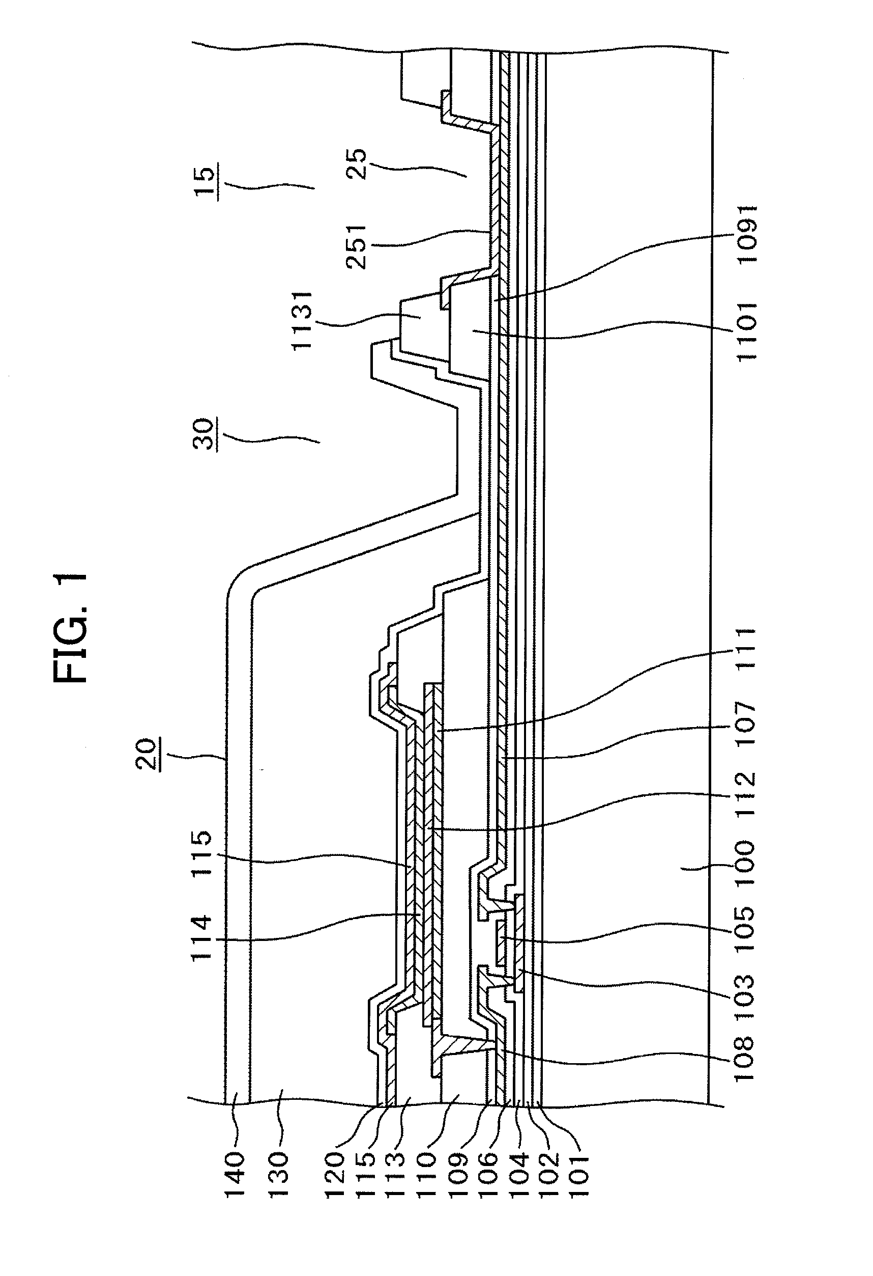
[0024]According to the aspects of the invention, in the solid-sealing type organic EL display device, it is possible to prevent voids or cracks from being generated in the inorganic passivation film formed over the extraction line in the peripheral sealing region around the display region. Consequently it is possible to prevent the organic EL layer from being deteriorated by water and the appearance of the dark area can be prevented in the organic EL display device.

Problems solved by technology

Luminescence properties are deteriorated when water exists in an organic EL material of the organic EL display device, and the area where the luminescence properties are deteriorated due to water will stop emitting light eventually while the device is operated for a long period of time.
The dark spot grows as time advances and results in an image defect.
However, the hollow-sealing type organic EL display device has disadvantages that adjustment of a gap between the element substrate and the sealing substrate is difficult, the sealant which adhesively bonds the element substrate with the sealing substrate at their peripheral must have a large width in order to prevent water from intruding inside, an organic EL material can be contaminated with a gas emitted from the sealant when the substrate is sealed with the sealant, throughput is low and so forth.
Moreover, another disadvantage in a completed EL display device is that the organic EL layer can be damaged when the element substrate and the sealing substrate contact each other by an external force applied to the element substrate or the sealing substrate.
However, even when the peripheral sealing region is formed of an inorganic film alone, if a defect such as void exists in the inorganic film, water enters through the defect into a display region where is close to a terminal region and resulting in a dark area.
The inorganic passivation film and the like are fabricated through a low-temperature chemical vapor deposition (CVD) such as a plasma CVD, and it is difficult to eliminate defects such as voids completely.

Method used


Image

  • Organic el display device
  • Organic el display device
  • Organic el display device

Examples


first embodiment

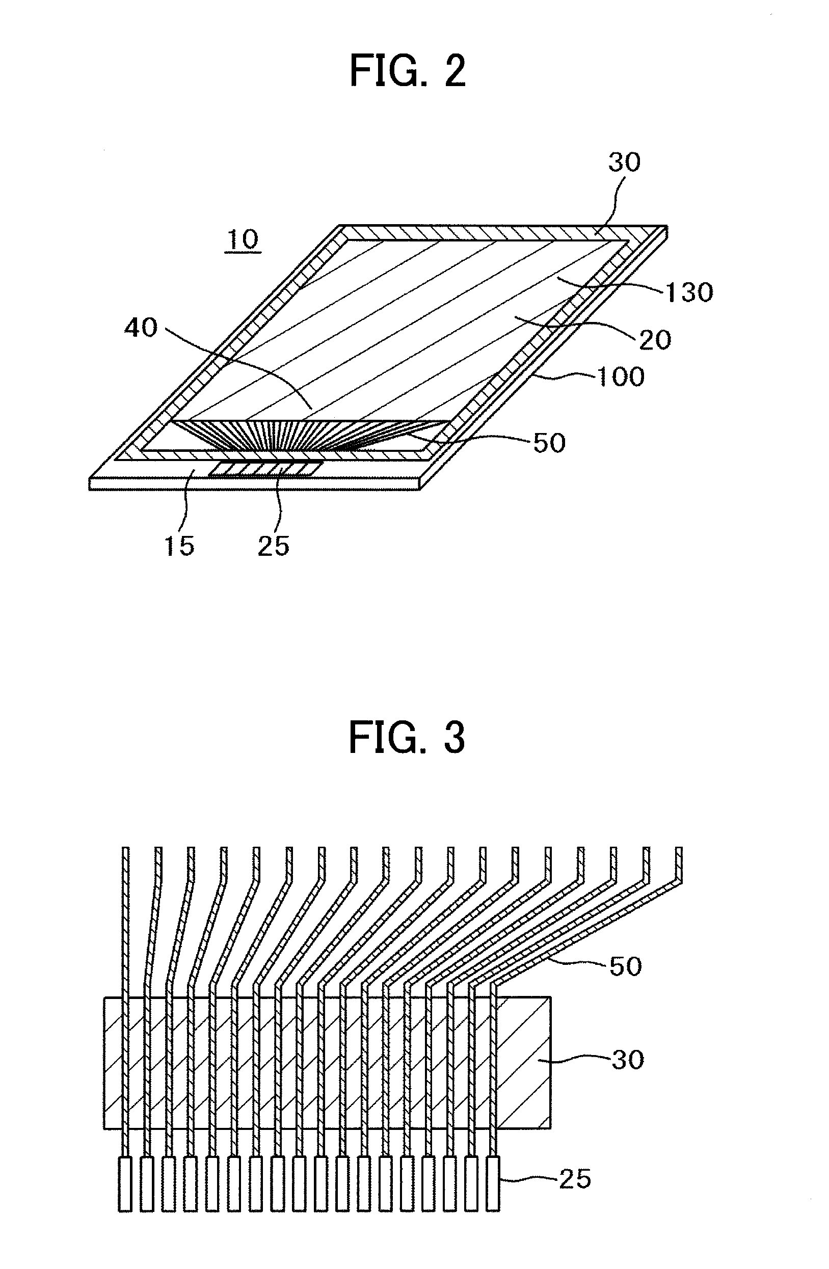
[0059]FIG. 4 is a plan view showing a configuration of the extraction line 50 in the peripheral sealing region 30 according to a first embodiment of the invention. Referring to FIG. 4, the extraction line 50 here is, for example, an extraction line of the image signal line. In the structure illustrated in FIG. 4, a pitch of the terminal is smaller than a pitch of the image signal line in the display region 20. In FIG. 4, the extraction line 50 extended from the display region 20 bends twice, at a first flexure part 51 and at a second flexure part 52.

[0060]The inorganic passivation film is formed by depositing SiN in a requisite amount through a low-temperature chemical vapor deposition (CVD) such as a plasma CVD and a pyrolytic CVD using a tungsten wire as catalyst. In this step, a large amount of the inorganic passivation films are fabricated in a short time period in order to improve the throughput, therefore it is prone to defect such as void. An example of a void 60 is illustrat...

second embodiment

[0072]In the first embodiment, the extraction line 50 is bent at 90 degrees in the crank shape in the peripheral sealing region 30. However, the extraction line 50 is not necessarily bent at 90 degrees in order to prevent the void 60 from stretching in the inorganic passivation film and to prevent the crack from further developing in the inorganic passivation film.

[0073]FIG. 10 illustrates an example in which a single extraction line 50 is bent at an angle larger than 90 degrees. In other words, the angle θ shown in FIG. 10 is 90 degrees according to the first embodiment but the angle is larger than 90 degrees according to the second embodiment. Even in this case, the wide open parts at the first flexure part 51 and the second flexure part 52, in other words, the sides of the flexure parts at the angle (360−θ), can hamper the progress of the void 60 and the crack from the peripheral sealing region 30 along the extraction line 50.

[0074]According to the experiments, the flexure part h...


PUM


Abstract

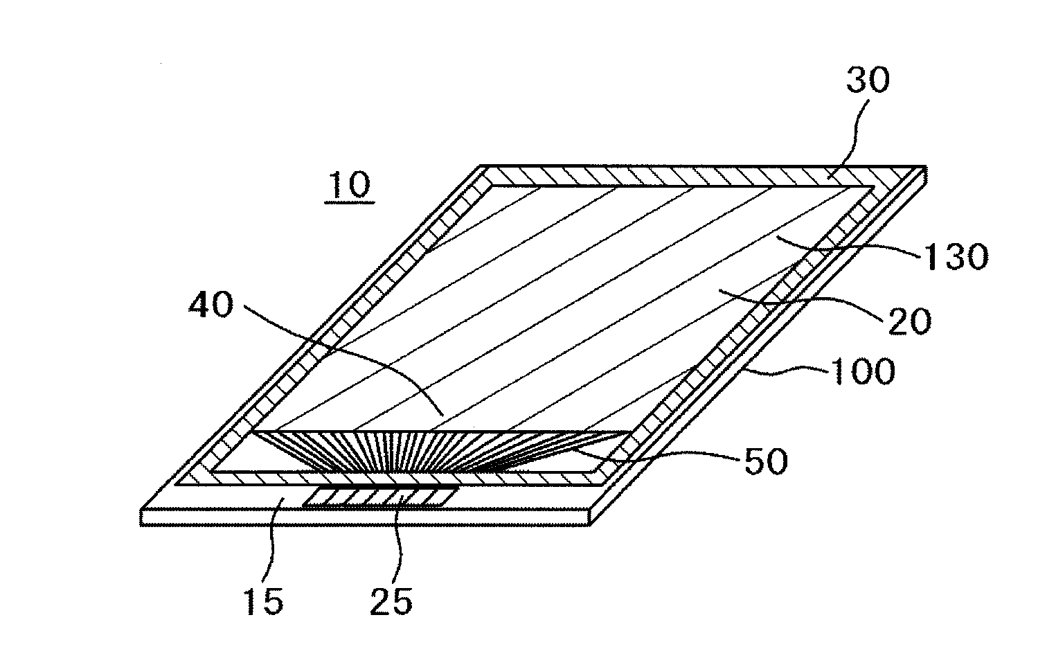
A solid-sealing type organic EL display device is provided that can prevent water permeation through a defect generated in a passivation film which covers an extraction line in a peripheral sealing region thereby making it possible to prevent deterioration of an organic EL layer. An extraction line that couples a wiring line in a display region with a terminal part passes a peripheral sealing region. The extraction line is covered with an inorganic passivation film in the peripheral sealing region. The extraction line has a first flexure part and a second flexure part in the peripheral sealing region thereby making it possible to prevent a void and a crack generated in the inorganic passivation film from penetrating the peripheral sealing region. Consequently it is possible to prevent water permeation from outside and to prevent the deterioration of the organic EL layer.

Description

CLAIM OF PRIORITY[0001]The present application claims priority from Japanese Patent Application JP 2009-160729 filed on Jul. 7, 2009, the content of which is hereby incorporated by reference into this application.BACKGROUND OF THE INVENTION[0002]1. Technical Field[0003]The present invention relates to an organic electro-luminescence (EL) display device, particularly a highly reliable organic EL display device in which appearance of dark areas due to water is prevented.[0004]2. Related Art[0005]In an organic EL display device, an organic EL layer is interposed between a lower electrode and an upper electrode. Luminescence of the organic EL layer is controlled by applying a fixed voltage to the upper electrode and applying a data signal voltage to the lower electrode. The data signal voltage is supplied to the lower electrode through a thin film transistor (TFT). The organic EL layer emits red, green or blue light depending on a material of an emissive layer. A pixel including such or...

Claims


Application Information

Patent Timeline
Patent Type & Authority Applications(United States)
IPC IPC(8): G09G3/30
CPCH01L27/3276H01L2251/5315H01L51/5253H01L51/5234H10K59/131H10K2102/3026H10K59/873H10K59/80524H10K50/844H10K50/828
Inventor TANAKA, MASAHIRO
Owner HITACHI DISPLAYS
Learn More