NAND flash memory

a technology of flash memory and nand flash, applied in the field of nand flash memory, can solve the problems of affecting the performance of the device, and the possibility of false writing of the device into an unselected memory cell transistor

Inactive Publication Date: 2011-01-13
KK TOSHIBA
View PDF1 Cites 26 Cited by
  • Summary
  • Abstract
  • Description
  • Claims
  • Application Information

AI Technical Summary

Problems solved by technology

This results in a problem that the yield falls.
However, the conventional method has a problem that writing into an unselected memory cell transistor might be falsely conducted (the threshold voltage might rise) if the intermediate voltage becomes high.

Method used


Image

  • NAND flash memory
  • NAND flash memory
  • NAND flash memory

Examples


first embodiment

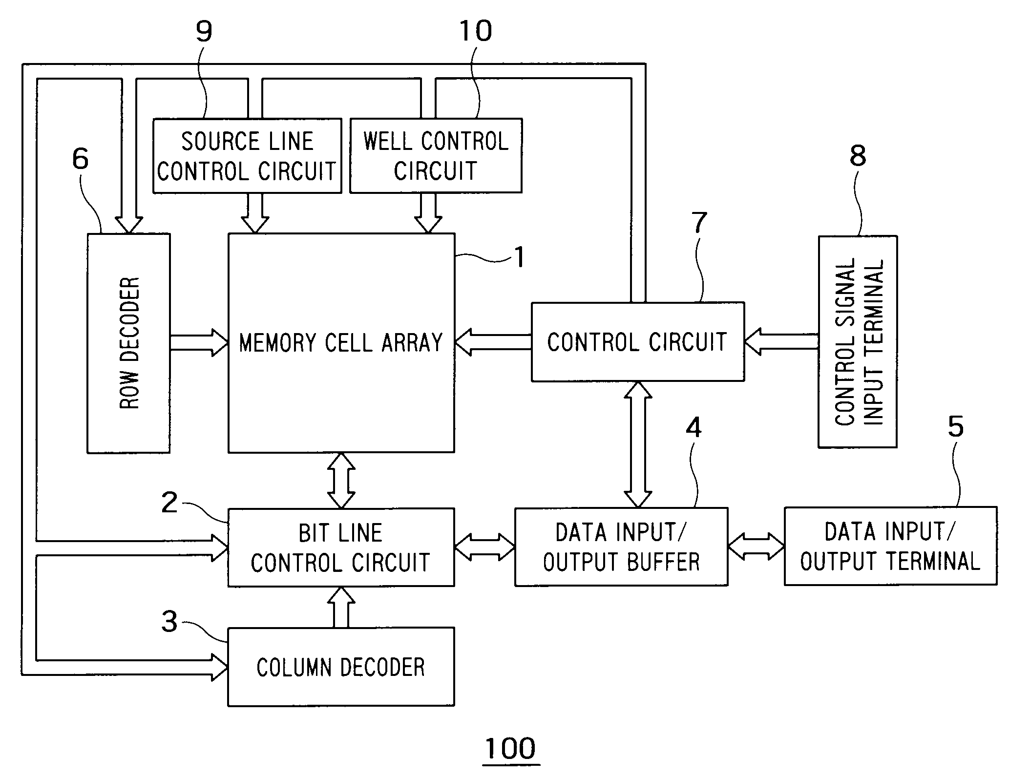
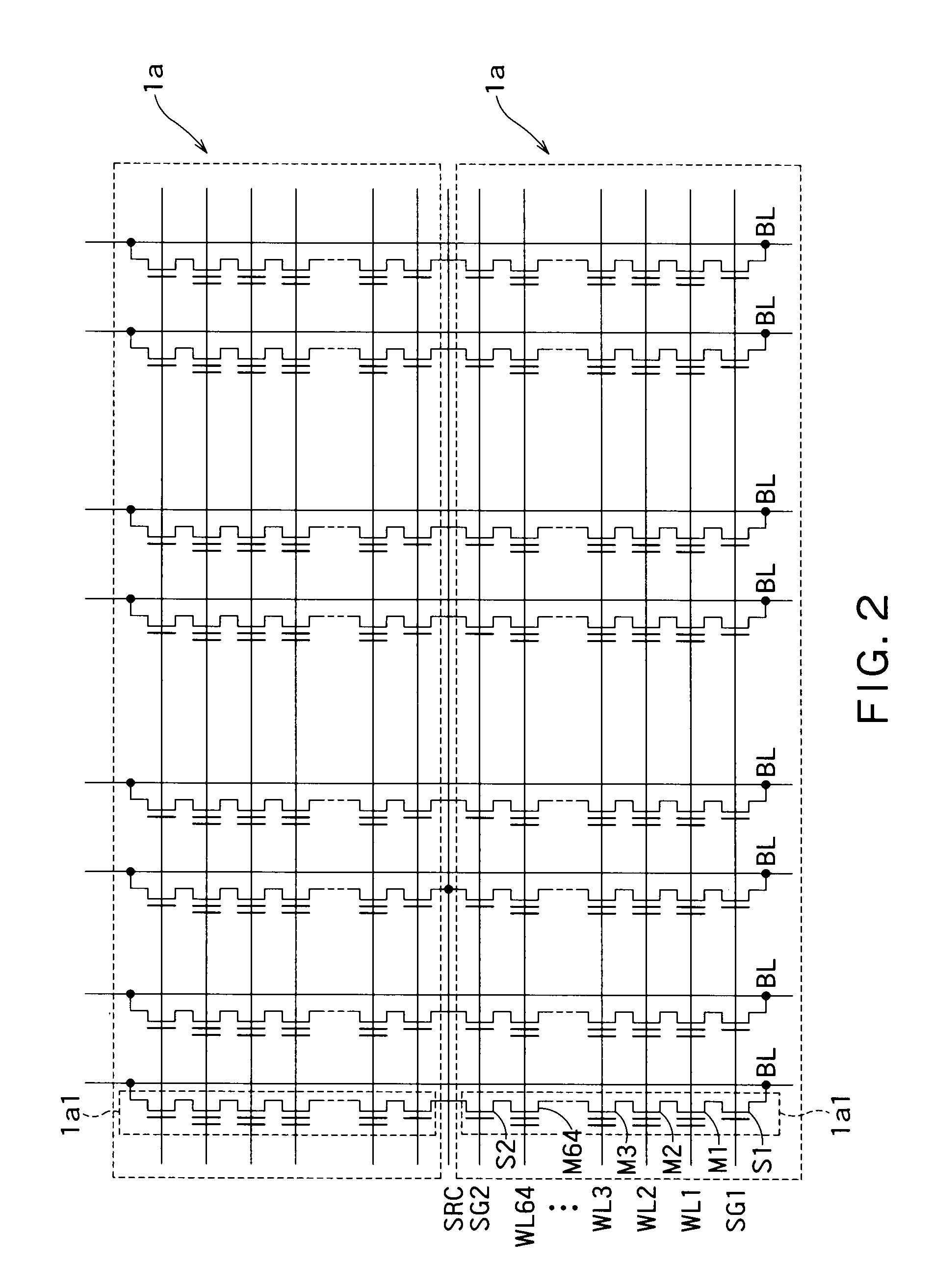
[0047]FIG. 1 is a block diagram showing an example of a NAND flash memory 100 according to a first embodiment, which is a mode of the present invention. FIG. 2 is a circuit diagram showing a configuration of a memory cell array shown in FIG. 1.

[0048]As shown in FIG. 1, the NAND flash memory 100 includes a memory cell array 1, a bit line control circuit 2, a column decoder 3, a data input / output buffer 4, a data input / output terminal 5, a row decoder 6, a control circuit 7, a control signal input terminal 8, a source line control circuit 9, and a well control circuit 10.

[0049]The memory cell array 1 includes a plurality of bit lines BL, a plurality of word lines WL, and a common source line SRC. In the memory cell array 1, for example, memory cell transistors M in which data can be electrically rewritten are arranged in a matrix form.

[0050]The bit line control circuit 2 for controlling voltages on the bit lines BL and the row decoder for controlling voltages on the word lines WL are ...

second embodiment

[0115]In the first embodiment, the case where the intermediate voltage Vpass is raised when the number n of times of looping of the program loop is the prescribed number na of times has been described.

[0116]In the present second embodiment, the case where the intermediate voltage Vpass is raised when the program voltage Vpgm is equal to a prescribed voltage Va will be described. By the way, the present second embodiment is applied to the NAND flash memory 100 according to the first embodiment shown in FIGS. 1 to 7 in the same way.

[0117]An example of a program loop of the NAND flash memory 100 according to the second embodiment will now be described.

[0118]FIG. 12 is a flow chart showing an example of a program loop of the NAND flash memory 100 according to the second embodiment. FIG. 13 is a waveform diagram showing an example of waveforms of the program voltage Vpgm and the intermediate voltage Vpass in the case where the program voltage Vpgm is set in the neighborhood of a program ...


PUM


Abstract

A NAND flash memory has memory cell transistors which data is written into. If number of times the program operation has been executed is not equal to the prescribed upper limit number of times, then the program voltage is set so as to be raised by a first potential difference and then the program operation and the verify operation are executed again, andonly when the number of times of the program operation has become equal to a prescribed number of times being less than the upper limit number of times, the intermediate voltage is raised by a second potential difference and fixed.

Description

CROSS-REFERENCE TO RELATED APPLICATION[0001]This application is based upon and claims the benefit of priority from the prior Japanese Patent Application No. 2009-162515, filed on Jul. 9, 2009, the entire contents of which are incorporated herein by reference.BACKGROUND OF THE INVENTION[0002]1. Field of the Invention[0003]The present invention relates to NAND flash memories in which data is written into memory cell transistors.[0004]2. Background Art[0005]In some conventional NAND flash memories, program operations and verify operations are repeated while raising the program voltage Vpgm applied to the control gate of a selected memory cell transistor stepwise every program loop (see, for example, JP-A 2008-47278 (KOKAI)). As a result, threshold voltages of memory cell transistors having dispersion in write characteristics are written into the same threshold voltages as far as possible.[0006]In the conventional NAND flash memories, writing is stopped on the way for a memory cell in w...

Claims


Application Information

Patent Timeline
Patent Type & Authority Applications(United States)
IPC IPC(8): G11C16/06
CPCG11C11/5628G11C2211/5621G11C16/3459
Inventor UENO, KOKIUCHIUMI, SATOSHI
Owner KK TOSHIBA
Why Eureka
Try Eureka