Optoelectronic device and method of making same
- Summary
- Abstract
- Description
- Claims
- Application Information
AI Technical Summary
Benefits of technology
Problems solved by technology
Method used
Image
Examples
Embodiment Construction
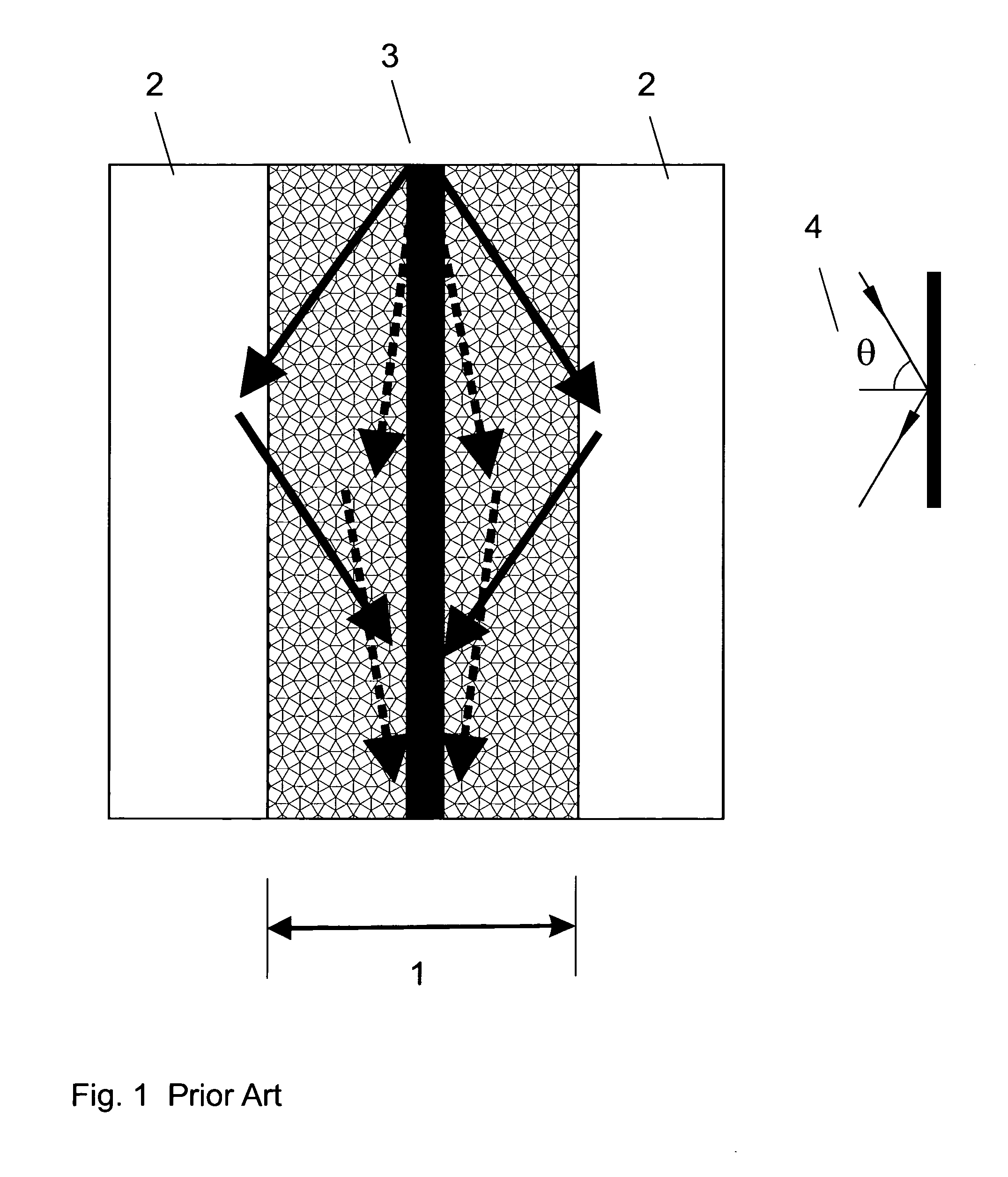
[0018]A schematic representation of the prior art device is shown in FIG. 1. It represents a medium (1) placed in the waveguide region confined at least on one side by a reflector region (2). A layer composed of a certain medium (1) can be clad, for example, by evanescent reflectors (2) composed of layers having a lower refractive index as compared to the medium. A gain region (3) is introduced inside the medium may interact with different optical waves existing in the device once the geometrical dimensions of the medium region is large enough to support several optical modes at different effective mode angles. Unless the gain medium has a particular width and specially placed with respect to one or another waveguide mode, all the optical modes may have a significant overlap with the gain region and be amplified.
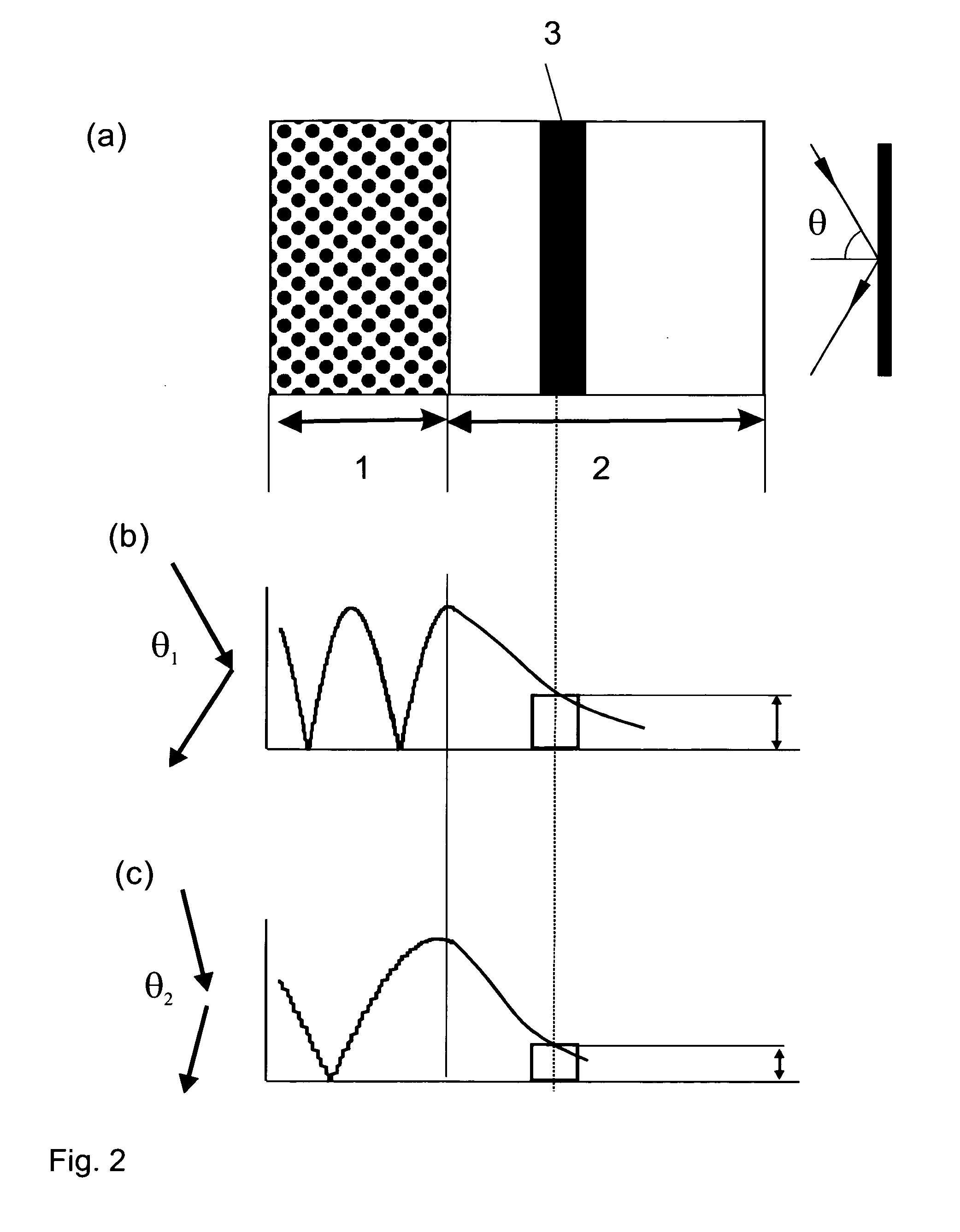
[0019]In the device proposed in the present invention, which is schematically represented in FIG. 2 (a) the gain medium (3) is incorporated deeply into the layer of the evan...
PUM
 Abstract
Description
Claims
Application Information


