Light-emitting element and method of fabricating the same

a technology of light-emitting elements and light-emitting elements, which is applied in the direction of electroluminescent light sources, semiconductor/solid-state device details, electric lighting sources, etc., can solve the problems of deteriorating optical efficiency of light-emitting elements, and achieve the effects of improving optical efficiency, increasing the utilization of active layers, and increasing current in light-emitting structures

Active Publication Date: 2011-01-20
SAMSUNG ELECTRONICS CO LTD
View PDF5 Cites 78 Cited by
  • Summary
  • Abstract
  • Description
  • Claims
  • Application Information

AI Technical Summary

Benefits of technology

[0008]Example embodiments of the present invention provide a light-emitting element in which spreading of a current in a light-emitting structure is increased and / or maximized to increase utilization of an active layer and to improve optical efficiency.

Problems solved by technology

Accordingly, light may be generated in only part of the light-emitting pattern, thereby deteriorating optical efficiency of the light-emitting element.

Method used


Image

  • Light-emitting element and method of fabricating the same
  • Light-emitting element and method of fabricating the same
  • Light-emitting element and method of fabricating the same

Examples


Embodiment Construction

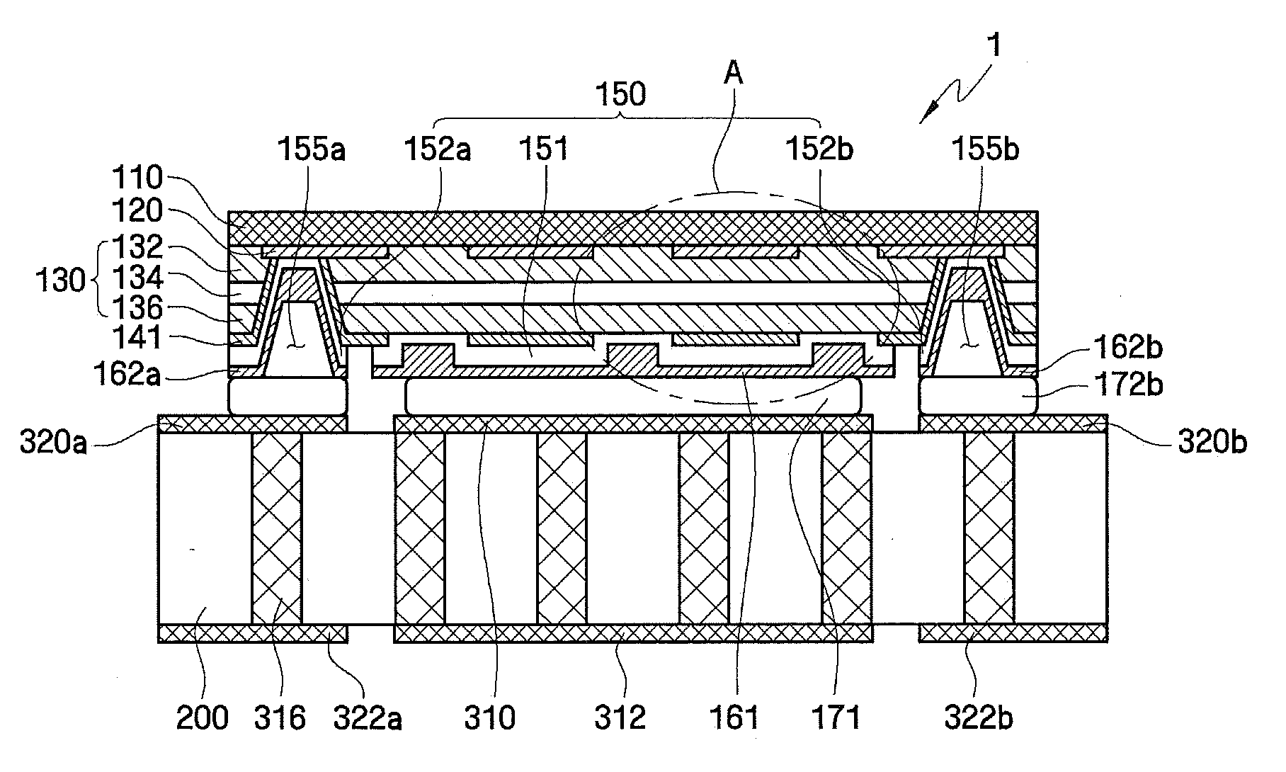
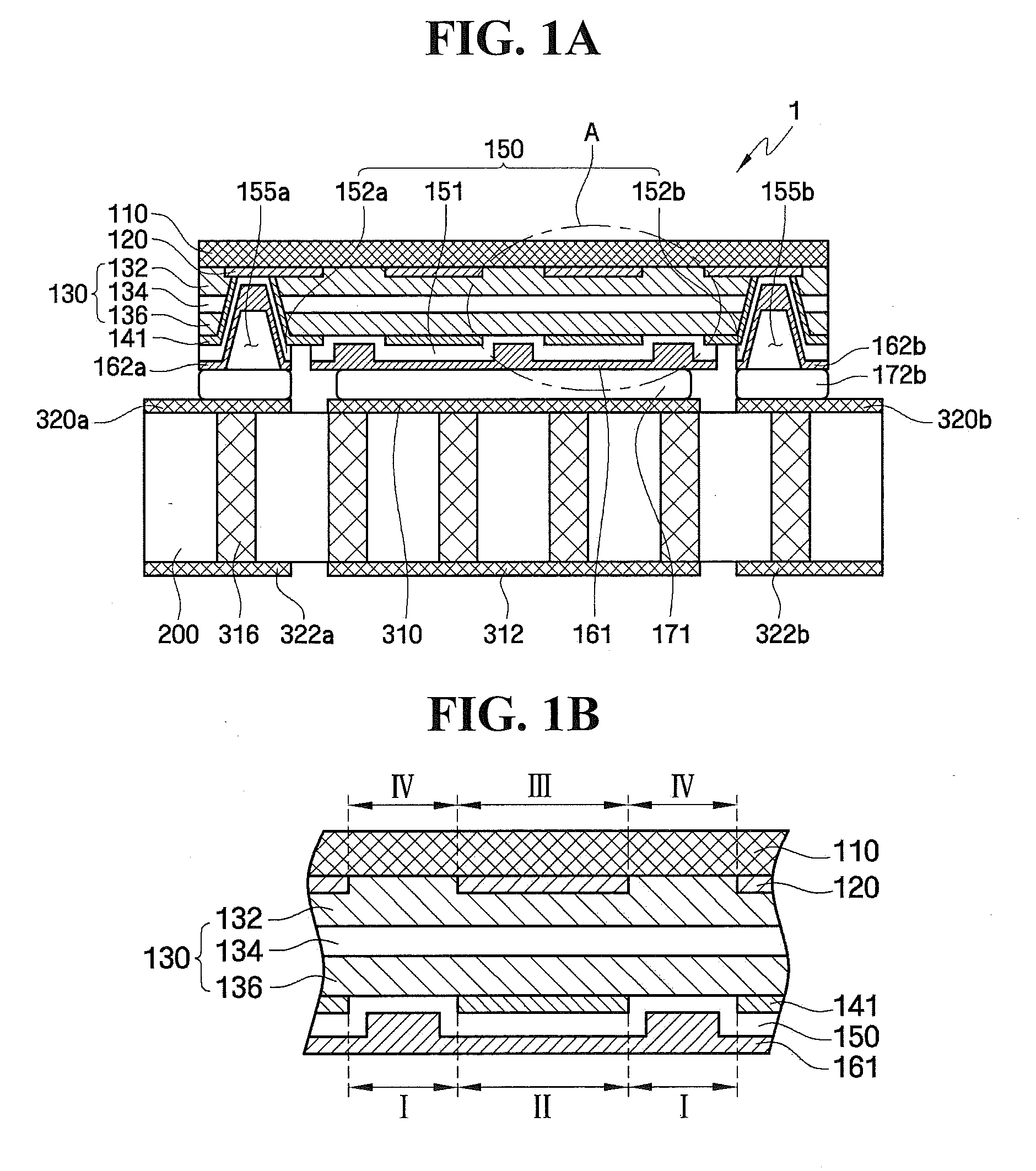
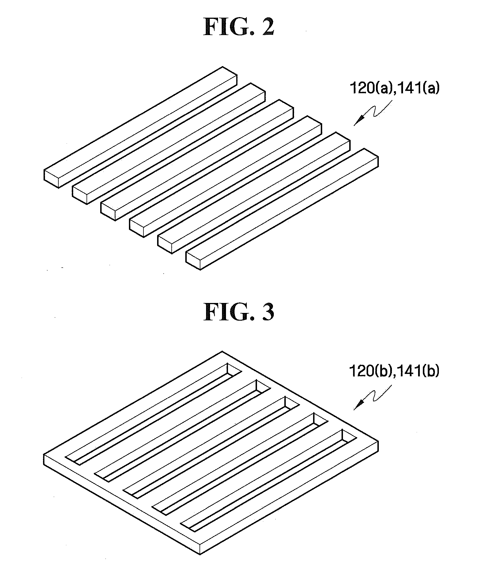
[0024]Advantages and features of the present invention and methods of accomplishing the same may be understood more readily by reference to the following detailed description of exemplary embodiments and the accompanying drawings. The present invention may, however, be embodied in many different forms and should not be construed as being limited to the embodiments set forth herein. Rather, these embodiments are provided so that this disclosure will be thorough and complete and will fully convey the concept of the invention to those skilled in the art, and the present invention will only be defined by the appended claims. In the drawings, sizes and relative sizes of layers and regions may be exaggerated for clarity.

[0025]The terminology used herein is for the purpose of describing particular embodiments only and is not intended to be limiting of the invention. As used herein, the singular forms “a”, “an” and “the” are intended to include the plural forms as well, unless the context c...


PUM


Abstract

Provided are a light-emitting element and a method of fabricating the same. The light-emitting element includes: a first pattern including conductive regions and non-conductive regions. The non-conductive regions are defined by the conductive regions. The light-emitting element also include an insulating pattern including insulating regions and non-insulating regions which correspond respectively to the conductive regions and non-conductive regions. The non-insulating regions are defined by the insulating regions. The light-emitting element further includes a light-emitting structure interposed between the first pattern and the insulating pattern. The light-emitting structure includes a first semiconductor pattern of a first conductivity type, a light-emitting pattern, and a second semiconductor pattern of a second conductivity type which are stacked sequentially. The light-emitting element also includes a second pattern formed in the non-insulating regions.

Description

[0001]This application claims priority to Korean Patent Application No. 10-2009-0065947, filed on Jul. 20, 2009, in the Korean Intellectual Property Office, the disclosure of which is incorporated herein by reference in its entirety.BACKGROUND[0002]1. Field of the Invention[0003]Example embodiments relate to a light-emitting element and a method of fabricating the same. More particularly, example embodiments relate to a light-emitting element and a method of fabricating the same, in which spreading of a current in a light-emitting structure is increased or maximized to increase utilization of an active layer and to improve optical efficiency.[0004]2. Description of the Related Art[0005]Light-emitting elements such as light-emitting diodes (LEDs) emit light when electrons combine with holes. Light-emitting elements have lower power consumption, have a long life, are installable in a limited space, and are resistant to vibrations.[0006]A light-emitting element may include a p electrod...

Claims


Application Information

Patent Timeline
Patent Type & Authority Applications(United States)
IPC IPC(8): H01L33/62
CPCH01L25/0753H01L33/382H01L33/387H01L33/42H01L33/14H01L2933/0016Y10S257/918H01L2224/16H01L33/62H01L33/0093H05B33/14
Inventor KIM, YU-SIK
Owner SAMSUNG ELECTRONICS CO LTD
Why Eureka
Try Eureka