Differential switch, d/a converter, semiconductor integrated circuit and communication apparatus

Active Publication Date: 2011-01-20
PANASONIC CORP
View PDF2 Cites 8 Cited by
  • Summary
  • Abstract
  • Description
  • Claims
  • Application Information

AI Technical Summary

Benefits of technology

[0038]The present invention prevents fluctuations in voltage at a common source node in a differential switch circuit. The use of the diff

Problems solved by technology

This causes noise dependent on the input digital code, and affect

Method used


Image

  • Differential switch, d/a converter, semiconductor integrated circuit and communication apparatus
  • Differential switch, d/a converter, semiconductor integrated circuit and communication apparatus
  • Differential switch, d/a converter, semiconductor integrated circuit and communication apparatus

Examples


embodiment 1

(Structure of D / A Converter 100)

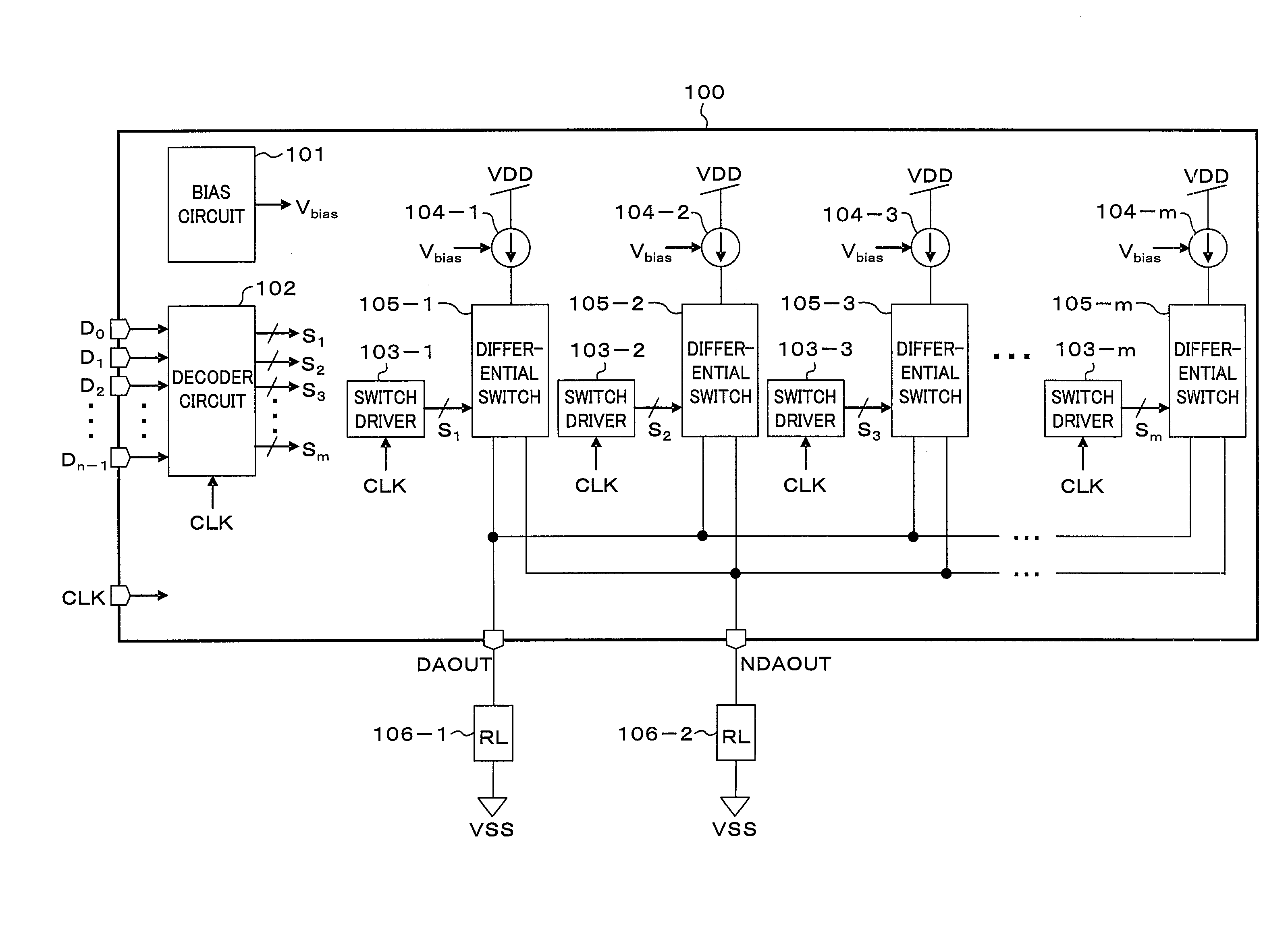
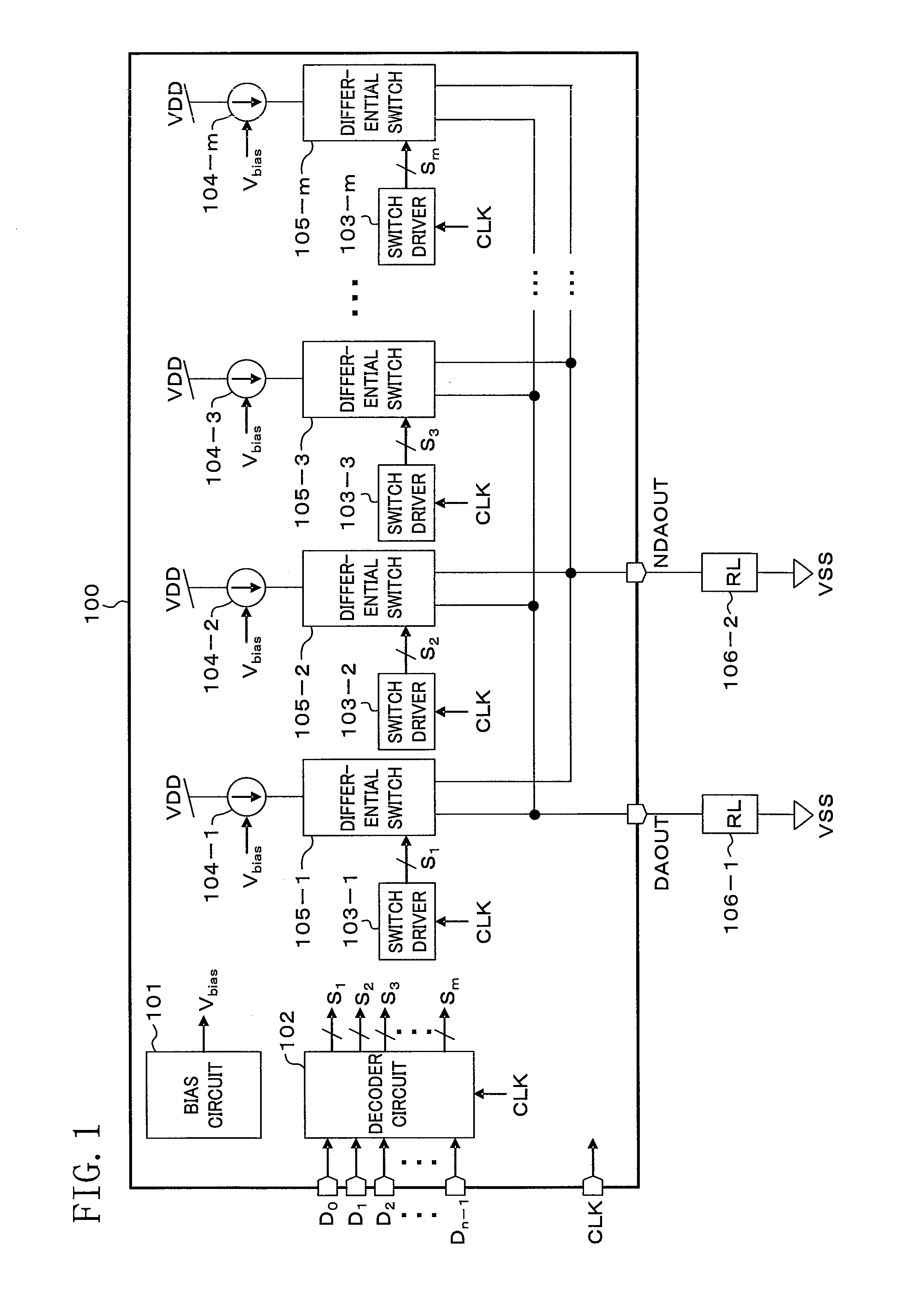
[0059]FIG. 1 is a block diagram illustrating a D / A converter 100 according to the first embodiment. The D / A converter 100 outputs analog output current signals, which are converted from n-bit digital signals D0 through Dn-1 input from the outside to analog signals, from an analog non-inverting output terminal DAOUT. The D / A converter 100 outputs inverted signals of the analog output current signals from an analog inverting output terminal NDAOUT. Load resistors (RL) 106-1 and 106-2 are coupled to the analog non-inverting output terminal DAOUT and the analog inverting output terminal NDAOUT, respectively. Analog output current signals output from the output terminals DAOUT and NDAOUT are converted into voltages by the load resistors 106-1 and 106-2 for current-voltage conversion. As a result, analog output voltages according to the input digital signals D0 through Dn-1 can be obtained.

[0060]The D / A converter 100 includes a bias circuit 101, a decoder c...

embodiment 2

[0078]A D / A converter 100 according to the second embodiment has a similar overall structure as shown in FIG. 1, but includes a current switch of FIG. 4 instead of the current switch of FIG. 2.

(Structure of Current Switch)

[0079]FIG. 4 is a circuit diagram illustrating a current switch including a current source 104-1 and a differential switch circuit 105-1. Note that FIG. 4 also represents the circuit diagram of each current switch including a current source 104-i (where i ranges from 2 to m) and a differential switch circuit 105-i (where i ranges from 2 to m).

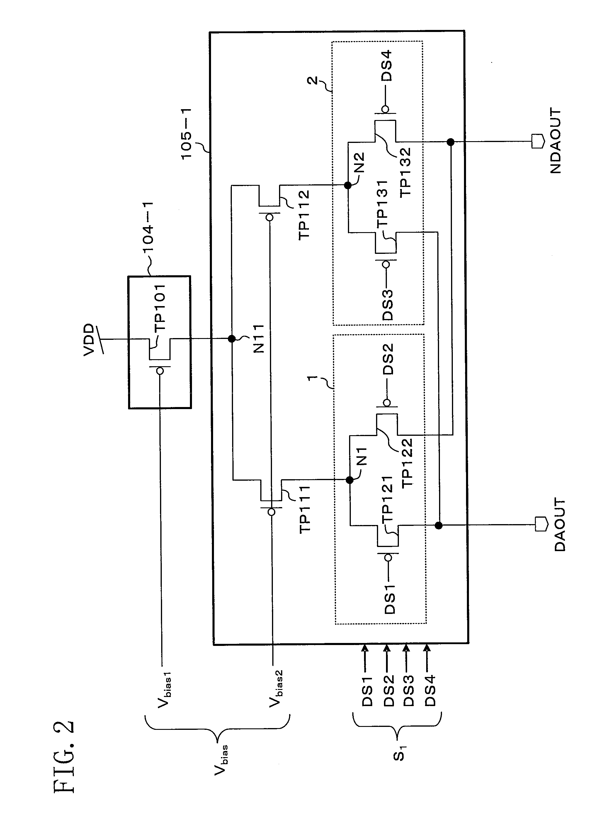
[0080]In the current switch of FIG. 4, the current source 104-1 includes a current source transistor TP101 and a cascode transistor TP102. The differential switch circuit 105-1 includes cascode transistors TP111 and TP112, and differential switch basic circuits 1 and 2. A bias voltage Vbias, which is output from the bias circuit 101 of FIG. 1, includes bias voltages Vbias1, Vbias2, and Vbias3. Each digital signal Si (where i r...

embodiment 3

[0085]A D / A converter according to the third embodiment has a similar overall structure as shown in FIG. 1, but includes a current switch of FIG. 5 instead of the current switch of FIG. 2.

(Structure of Current Switch)

[0086]FIG. 5 is a circuit diagram illustrating a current switch including a current source 104-1 and a differential switch circuit 105-1. Note that FIG. 5 also represents the circuit diagram of each current switch including a current source 104-i (where i ranges from 2 to m) and a differential switch circuit 105-i (where i ranges from 2 to m).

[0087]In the current switch of FIG. 5, the current source 104-1 includes a current source transistor TP101. The differential switch circuit 105-1 includes cascode transistors TP111 and TP112, and differential switch basic circuits 1 and 2. A bias voltage Vbias, which is output from the bias circuit 101 of FIG. 1, includes bias voltages Vbias1 and Vbias2. Each digital signal Si (where i ranges from 1 to m), which is output from the ...


PUM


Abstract

A differential switch circuit includes a first differential switch basic circuit (1) and a second differential switch basic circuit (2). The first differential switch basic circuit (1) has a first common source node (N1) shared by a plurality of transistors (TP121 and TP122), and the second differential switch basic circuit (2) has a second common source node (N2) shared by a plurality of transistors (TP131 and TP132). The first common source node (N1) and the second common source node (N2) are alternately reset to a predetermined voltage in each clock cycle.

Description

TECHNICAL FIELD[0001]The present disclosure relates to differential switches for switching current channels, D / A converters (DAC) for converting digital signals into analog signals, semiconductor integrated circuits, and communication apparatuses. More particularly, the present disclosure relates to techniques for improving distortion characteristics in D / A converters.BACKGROUND ART[0002]In recent years, various wired or wireless communication systems have been researched and developed. Accordingly, D / A converters for higher speed communications having conversion rates of several hundreds MHz to several tens GHz have become essential. Since D / A converters for communications are particularly desired to have low distortion characteristics, various circuit techniques have been suggested. Current steering D / A converters capable of performing high speed operations are typically used as D / A converters for communications.[0003]FIG. 1 illustrates the overall structure of a conventional curr...

Claims


Application Information

Patent Timeline
IPC IPC(8): H03M1/66H03K17/56H03K17/687
CPCH03M1/747H03M1/0682H03K17/6871H03K17/162
Inventor IKOMA, HEIJI
Owner PANASONIC CORP
Why Eureka
Try Eureka