Phase element for introducing a phase shift pattern into an electromagnetic wave

a phase element and phase shift technology, applied in the field of phase or amplitude shifting elements, can solve the problems of significant decoupling of achievable phase and amplitude shift patterns, corresponding increase of transmission losses, etc., and achieve low amplitude shift, low cost, and increase of transmission losses

Inactive Publication Date: 2011-02-03
HER MAJESTY THE QUEEN & RIGHT OF CANADA REPRESENTED BY THE MIN OF IND THROUGH THE COMM RES CENT
View PDF6 Cites 23 Cited by
  • Summary
  • Abstract
  • Description
  • Claims
  • Application Information

AI Technical Summary

Benefits of technology

[0017]A phase element of the present invention generates a pattern of phase shifts using an approach similar to newspaper printing, where the grey tones are obtained from different size of small black dots in a given, predetermined array. Instead of the ink on paper used in the newspaper printing process, metallic patches are etched on a dielectric substrate layer. A single layer of metallic patches does not produce a significant phase shift range and is always associated with a considerable amplitude shift pattern dependent on the phase shift pattern. Accordingly, adding mor

Problems solved by technology

Accordingly, adding more thin dielectric layers has been initially expected to result in a corresponding increase of the transmission loss, which was undesired

Method used


Image

  • Phase element for introducing a phase shift pattern into an electromagnetic wave
  • Phase element for introducing a phase shift pattern into an electromagnetic wave
  • Phase element for introducing a phase shift pattern into an electromagnetic wave

Examples


Embodiment Construction

[0065]While the present teachings are described in conjunction with various embodiments and examples, it is not intended that the present teachings be limited to such embodiments. On the contrary, the present teachings encompass various alternatives, modifications and equivalents, as will be appreciated by those of skill in the art.

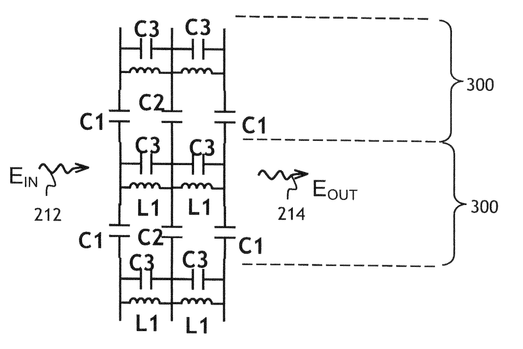
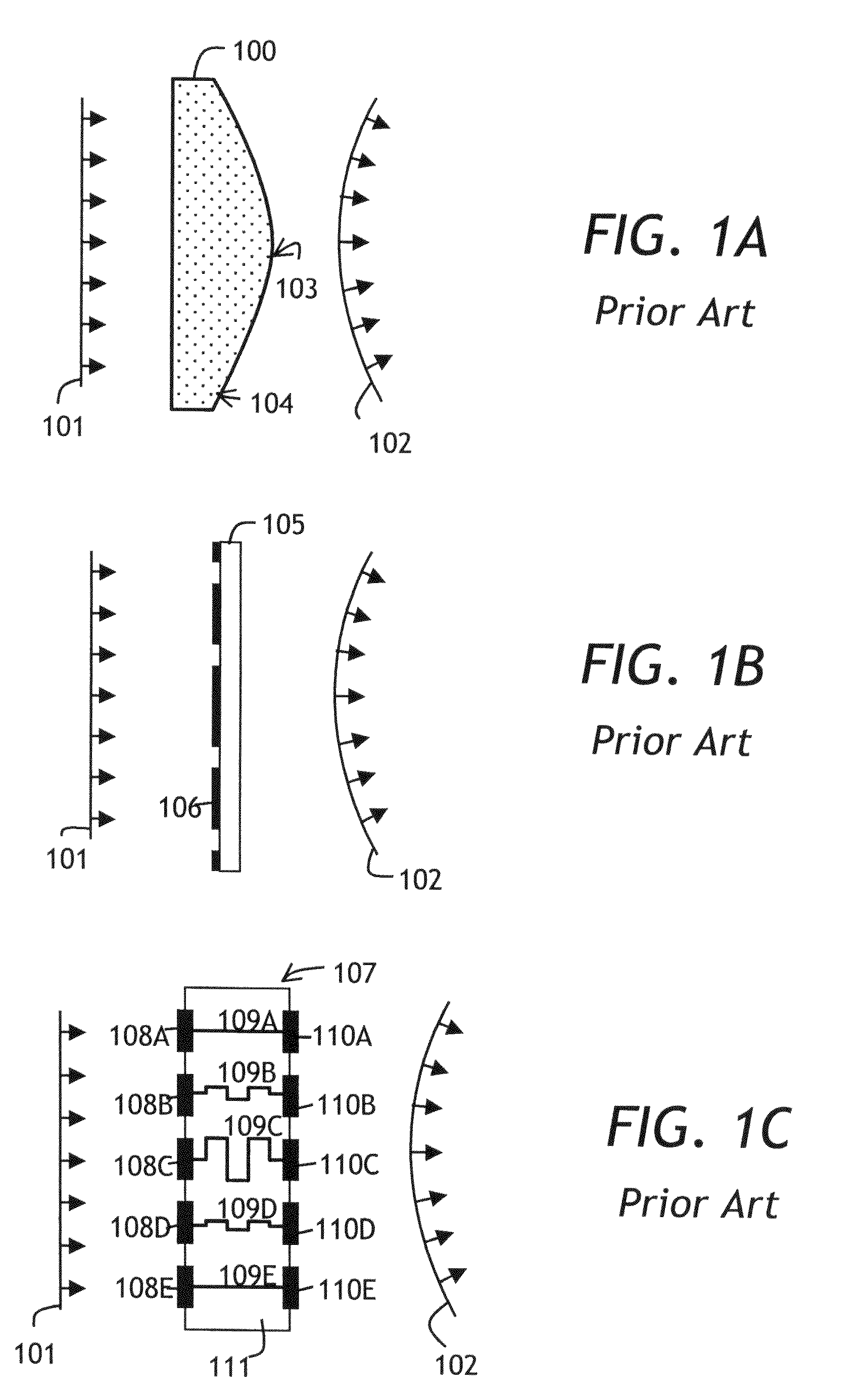
[0066]Throughout the specification, the phase element of the invention is called a “phase and amplitude shifting surface” (PASS) or a “phase shifting surface” (PSS). Herein, the word “surface” is used to refer to an “electrically thin” element, that is an element whose lateral dimensions are much smaller than a wavelength of the electromagnetic wave propagating through the element. The PSS is an element that alters phase distribution of the electromagnetic wave, while introducing a negligible transmission loss.

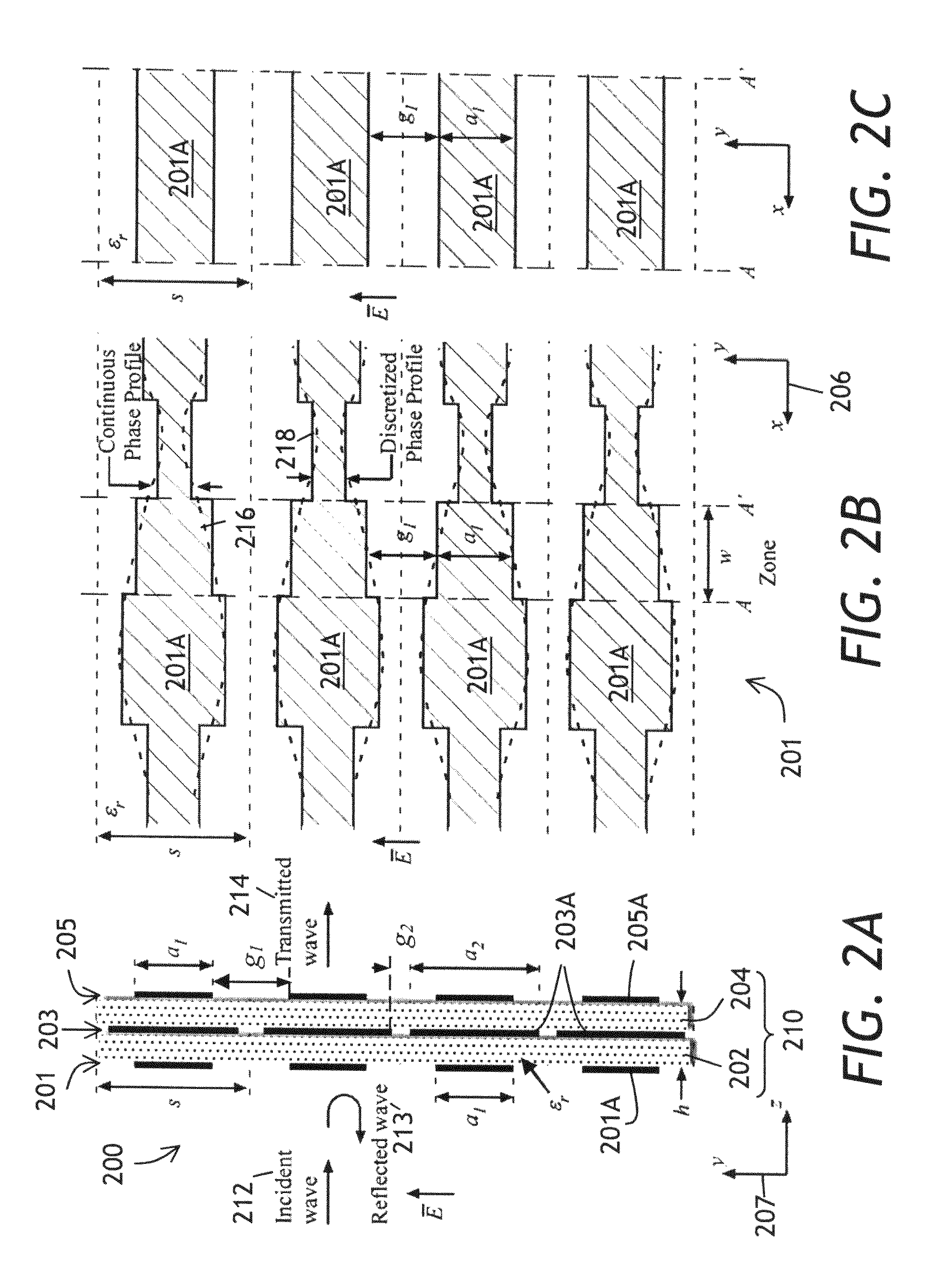
[0067]Referring to FIGS. 2A to 2C, a PSS, or a phase element 200 of the invention is shown in side and plan views. In FIG. 2A, a side cross-section...


PUM


Abstract

A thin electromagnetic phase shifting element, named phase and amplitude shifting surface (PASS), is disclosed. The PASS is capable of independently altering both the phase and the amplitude distribution of the electromagnetic fields propagating through the structure. The element comprises a few patterned metallic layers separated by dielectric layers. The patterns of the metallic layers are tuned to locally alter the phase and/or the amplitude of an incoming electromagnetic wave to a prescribed set of desired values for the outgoing electromagnetic wave. The PASS can be applied to design components such as gratings, lenses, holograms, and various types of antennas in the microwave, millimetre wave and sub-millimetre wave.

Description

CROSS-REFERENCE TO RELATED APPLICATIONS[0001]The present invention claims priority from U.S. Provisional Patent Application No. 61 / 230,180, filed Jul. 31, 2009, and Canadian Patent Application No. 2,674,785, filed Aug. 4, 2009, which are incorporated herein by reference.TECHNICAL FIELD[0002]The present invention relates to devices for altering a wavefront of an electromagnetic wave, and in particular to phase or amplitude shifting elements for redirecting, focusing, or collimating an electromagnetic wave.BACKGROUND OF THE INVENTION[0003]Electromagnetic waves are widely used in areas ranging from communication and radiolocation to TV broadcasting, imaging, medical treatment, and food processing. Electromagnetic waves in the microwave, millimeter-wave, and in sub-millimeter wave ranges are particularly useful for the purposes of communication due to relatively high carrier frequency and associated ease of beaming the wave and comparatively large information carrying capacity. Electrom...

Claims


Application Information

Patent Timeline
IPC IPC(8): H01P1/18B29D11/00
CPCH01Q15/0006H01Q15/10H01Q15/02H01Q15/0033H01Q19/06
Inventor GAGNON, NICOLASPETOSA, ALDOMCNAMARA, DEREK A.
Owner HER MAJESTY THE QUEEN & RIGHT OF CANADA REPRESENTED BY THE MIN OF IND THROUGH THE COMM RES CENT
Why Eureka
Try Eureka