Method for correcting layout pattern

a layout pattern and layout technology, applied in the field of layout pattern correction, can solve the problems of limiting the correction process from outputting a precise layout pattern, often occurring devices, and jeopardizing the performance of semiconductor devices, so as to reduce blind spots

Active Publication Date: 2011-02-03
UNITED MICROELECTRONICS CORP
View PDF8 Cites 23 Cited by
  • Summary
  • Abstract
  • Description
  • Claims
  • Application Information

AI Technical Summary

Benefits of technology

[0010]It is an objective of the present invention to provide a method for correcting lay...

Problems solved by technology

In the photolithographic step, deviations often occur and jeopardize the performance of the semiconductor device when the patterns on the masks are transferred onto the wafer surface.
The commercially available OPC software may test problems such as pitch, bridge, and critical dimension uniformity in the layout patterns.
Such methods not only test problems in the layout patterns but also correc...

Method used


Image

  • Method for correcting layout pattern
  • Method for correcting layout pattern
  • Method for correcting layout pattern

Examples


Embodiment Construction

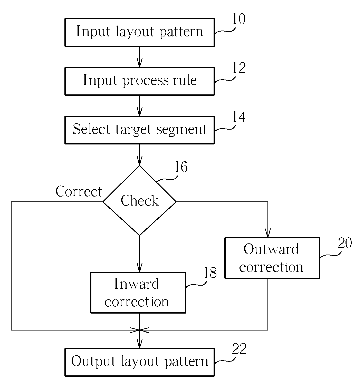
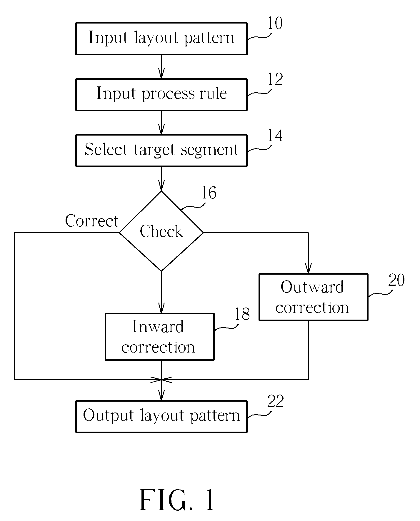
[0019]Referring to FIG. 1, FIG. 1 is a flow chart illustrating a method of correcting a layout pattern of the present invention. The method of verifying a layout pattern includes following steps. First, step 10 is carried out to input a preliminary layout pattern from a computer system, in which the layout pattern includes at least a segment. The layout pattern has preferably been corrected at least once by an optical proximity correction in the aforementioned computer system or other computer systems. The optical proximity corrections are prevalent correction methods used to modify widths, line ends and corners of each segment of a layout pattern in semiconductor industry. Next, step 12 is carried out to input a process rule. The process rule includes the critical width and the critical space or other design rules, which may derivate from the integrated circuits of the line width of 65 nm, 45 nm or below. Afterwards, step 14 is carried out to select a target segment and expand a ru...


PUM


Abstract

A method for correcting layout pattern is disclosed. The method includes the steps of: providing a layout pattern having at least one segment; forming a rule-checking rectangle from the segment, wherein the rule-checking rectangle comprises at least one square; verifying whether the square of the rule-checking rectangle overlaps other layout pattern; removing the portion of other layout pattern overlapped by the square to obtain a corrected layout pattern; and outputting the corrected layout pattern to a mask.

Description

BACKGROUND OF THE INVENTION[0001]1. Field of the Invention[0002]The invention relates to a method of correcting layout pattern, and more particularly, to a method of correcting layout pattern with no blind spot.[0003]2. Description of the Prior Art[0004]Critical technologies such as the photolithography and etching technologies are frequently used in semiconductor manufacturing processes. The photolithography technology usually involves transferring a complicated integrated circuit pattern to a semiconductor wafer surface for steps such as etching and implantation. These patterns must be extremely accurate for forming delicate integrated circuits so as to align with the patterns of the previous and following steps.[0005]In the photolithographic step, deviations often occur and jeopardize the performance of the semiconductor device when the patterns on the masks are transferred onto the wafer surface. Such deviations are usually related with the characters of the patterns to be trans...

Claims


Application Information

Patent Timeline
IPC IPC(8): G06F17/50
CPCG06F17/5081G06F30/398
Inventor YANG, YU-SHIANGHUANG, CHUN-HSIEN
Owner UNITED MICROELECTRONICS CORP
Why Eureka
Try Eureka