Microcavity structure and encapsulation structure for a microelectronic device

a microelectronic device and microcavity technology, applied in the direction of microstructural devices, microstructure technology, lamination, etc., can solve the problems of not being able to achieve a pressure less than about 10sup>3 /sup>mbar, risk of damage to the device or altering the proper operation, and not being able to fabricate release holes with dimensions larger than 5 m

Inactive Publication Date: 2011-02-10
COMMISSARIAT A LENERGIE ATOMIQUE ET AUX ENERGIES ALTERNATIVES
View PDF2 Cites 16 Cited by
  • Summary
  • Abstract
  • Description
  • Claims
  • Application Information

AI Technical Summary

Problems solved by technology

However, with this type of encapsulation procedure, even assisted by a getter deposited in the microcavity, it is difficult to attain a pressure less than about 10−3 mbar in the microcavity and therefore to control the residual atmosphere in the microcavity in which the microelectronic device is encapsulated.
However, even when the microelectronic device is not placed directly below the holes, there is still a risk of damaging the device or of altering its proper operation ...

Method used


Image

  • Microcavity structure and encapsulation structure for a microelectronic device
  • Microcavity structure and encapsulation structure for a microelectronic device
  • Microcavity structure and encapsulation structure for a microelectronic device

Examples


third embodiment

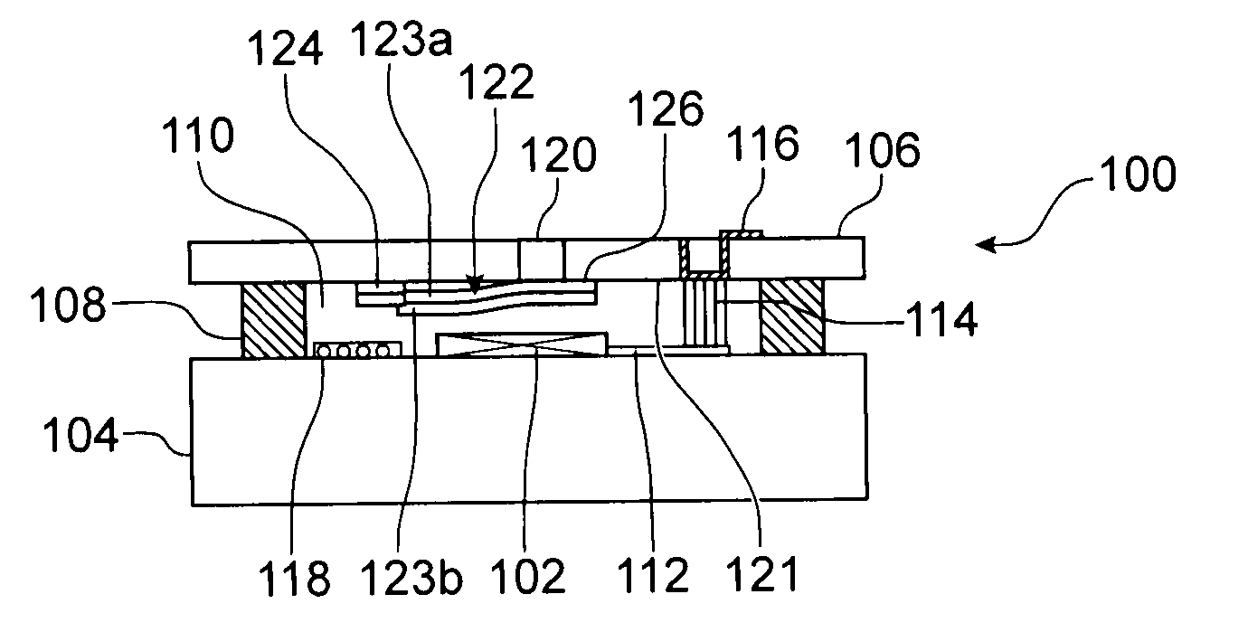
[0053]FIGS. 1, 3 and 4 show the microcavity structures serving as an encapsulation structure for a microelectronic device, respectively according to a first, a second and a third embodiment;

first embodiment

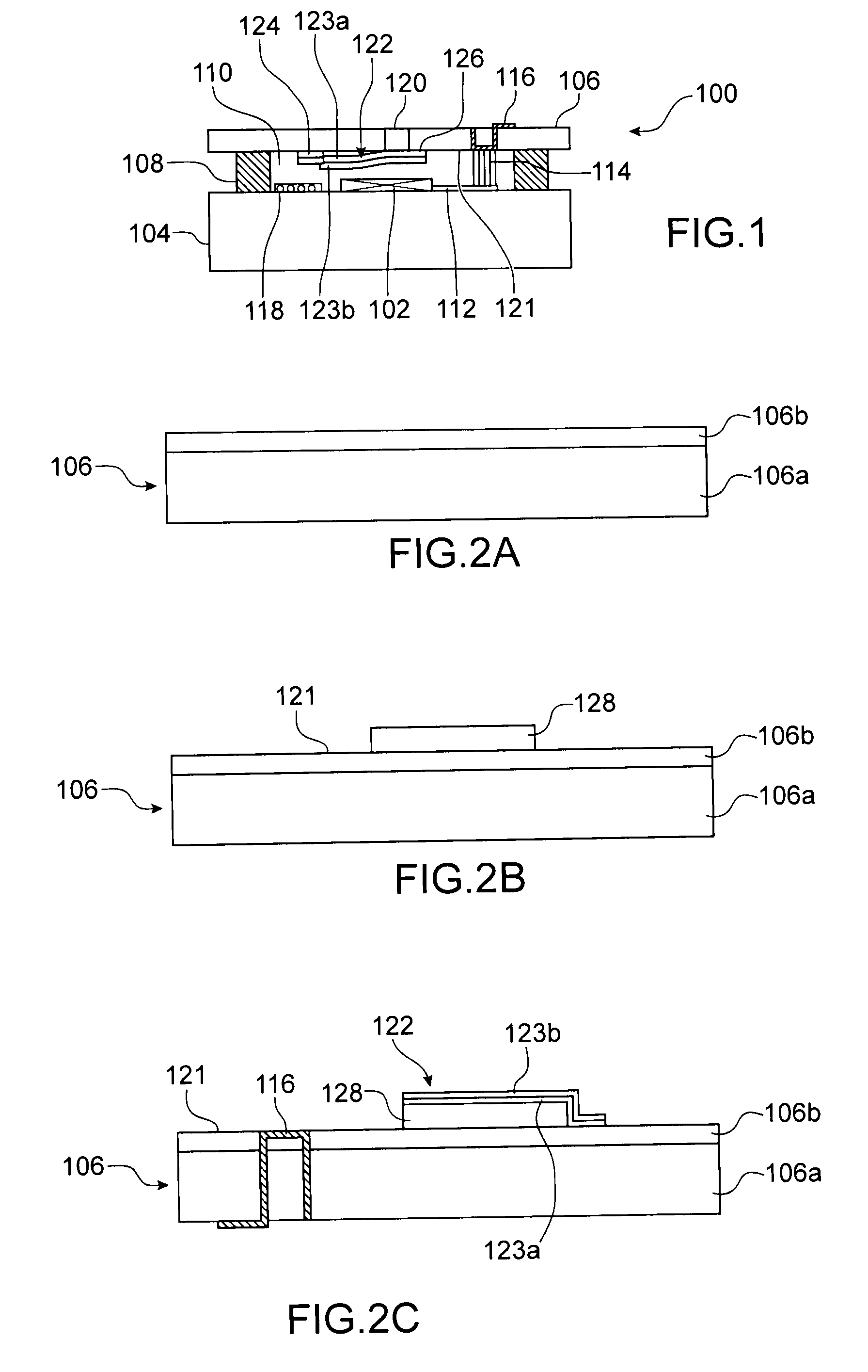
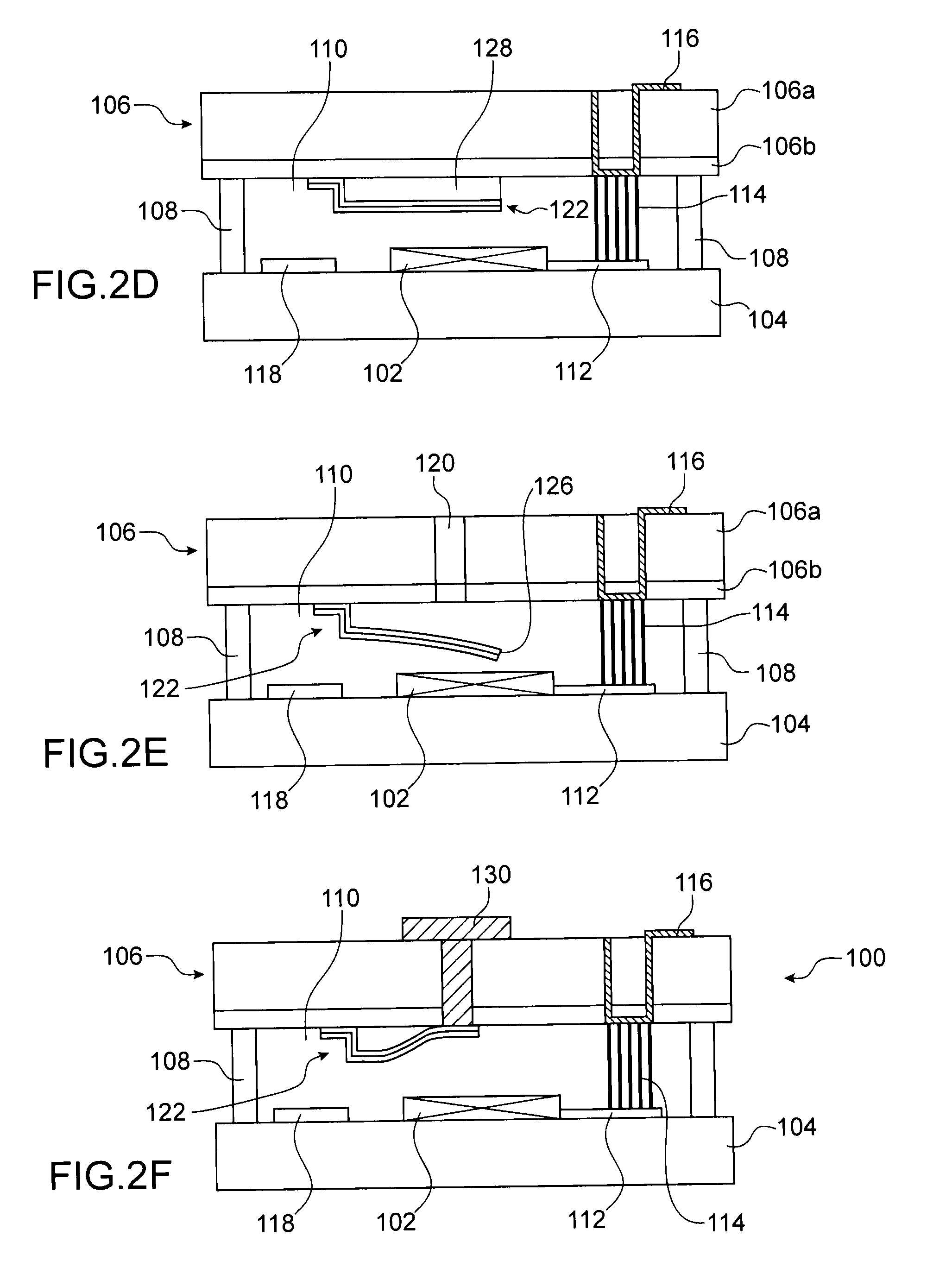
[0054]FIGS. 2A and 2F show the stages of a method of producing a microcavity structure corresponding to a method of encapsulation for a microelectronic device, ;

[0055]FIGS. 5A and 5F show the stages of a method of producing a microcavity structure corresponding to a method of encapsulation for a microelectronic device, according to the third embodiment;

[0056]FIG. 6 show an example of a closing flap for a microcavity structure.

[0057]Identical, similar or equivalent parts of the various figures described hereafter have the same numerical references so as to facilitate passing from one figure to another.

[0058]The different parts shown on the figures are not necessarily shown on a uniform scale, in order to make the figures clearer.

[0059]The different possibilities (variants and embodiments) should be understood as non-exclusive with respect to each other and can be combined one with another.

DETAILED DESCRIPTION OF PARTICULAR EMBODIMENTS

[0060]Reference is first made to FIG. 1 which show...

second embodiment

[0085]Reference is made to FIG. 3 which shows a microcavity structure 200, serving as an encapsulation structure for the microelectronic device 102, according to a

[0086]With respect to the encapsulation structure 100 shown in FIG. 1, the structure 200 comprises a second substrate 202, e.g. made of a semiconductor, such as silicon, forming a cover and attached to the first substrate 104 by direct sealing at the level of the interface 204. In this second embodiment, the structure 200 does not comprise a sealing cord between the two substrates 104, 202. In addition, in this second embodiment, the getter material 118 is not present inside the microcavity 110. The fixed end 124 of the closing flap 122 is electrically linked to an electrical contact 132. Thus the closing flap 122 may be actuated by heating using the Joule effect, obtained by intermediary of an electrical current applied to the electrical contact 132. In addition, when the closing flap 122 comprises one of these portions 1...


PUM

PropertyMeasurementUnit
Thicknessaaaaaaaaaa
Thicknessaaaaaaaaaa
Lengthaaaaaaaaaa

Abstract

Microcavity structure comprising:
    • a substrate,
    • a cover attached to the substrate such that a space formed between the cover and the substrate forms the microcavity,
    • at least one hole passing through the cover, and
    • at least one closing flap for the hole placed inside the microcavity and comprising at least two portions of materials with different thermal expansion coefficients placed one against the other, one first end of said two portions being mechanically linked to the cover, a second end of said two portions being free, and at least a part of the closing flap being placed opposite the hole, said two portions being suitable for closing or not the hole under the effect of a variation of temperature.

Description

TECHNICAL AREA[0001]The invention relates to microelectronics, and more particularly to the field of microcavity structures used, e.g. for packaging or encapsulating microelectronic devices e.g. of the type MEMS (Micro electro-mechanical systems) and / or NEMS (Nano electro-mechanical systems) and / or MOEMS (Micro opto-electro-mechanical systems) and / or NOEMS (Nano opto-electro-mechanical systems) to protect them from the external environment.PRIOR ART[0002]A first type of encapsulation method for the encapsulation of microelectronic devices consists of the transfer of a cover, formed by a substrate, on the support on which the devices are fabricated. This type of encapsulation method requires the machining of a cover prior to its assembly on the support. In order to control the atmosphere inside the microcavity, it is necessary to produce at the same time, a hermetic seal between the support and the cover, but also to deposit a thin film getter on the cover, generally at the bottom of...

Claims


Application Information

Patent Timeline
IPC IPC(8): H05K5/00B32B38/04B32B37/24
CPCB81C1/00293Y10T156/1057B81C2203/0145
Inventor BAILLIN, XAVIERCAPLET, STEPHANEHILT, THIERRY
Owner COMMISSARIAT A LENERGIE ATOMIQUE ET AUX ENERGIES ALTERNATIVES
Why Eureka
Try Eureka