Buffering circuit with reduced dynamic power consumption

a buffer circuit and dynamic power consumption technology, applied in the field of output buffer circuits, can solve the problems of large impact of single source driving circuit on the whole source driver chip, shorten the life overheating of the source driver chip, etc., and achieve the effect of reducing dynamic power consumption

Active Publication Date: 2011-02-10
HIMAX TECH LTD +1
View PDF14 Cites 15 Cited by
  • Summary
  • Abstract
  • Description
  • Claims
  • Application Information

AI Technical Summary

Benefits of technology

[0008]The present application describes an output buffering circuit for a driver device, an amplifier circuit, and a display device employing the output buffering circuit with reduced dynamic power consumption.

Problems solved by technology

The power consumption of a single source driving circuit therefore has a large impact on the whole source driver chip.
On the other hand, for applications of large-size LCDs (liquid crystal displays) that accompany relatively large panel loads and strict system specifications, power consumption is often considerable, which results in over-heating in the source driver chip and shortens the life of the source driver chip.
For the abovementioned and other reasons, to reduce the total power consumption of the conventional output buffer, especially the dynamic power consumption in charging and discharging process, in consideration of meeting other requirements such as sufficient driving ability for the display panel, simplicity of design and manufacture, and / or other characteristics of circuit structure and operation, has become an important development issue.

Method used


Image

  • Buffering circuit with reduced dynamic power consumption
  • Buffering circuit with reduced dynamic power consumption
  • Buffering circuit with reduced dynamic power consumption

Examples


Embodiment Construction

.”

BRIEF DESCRIPTION OF THE DRAWINGS

[0012]Features, aspects, and embodiments are described in conjunction with the attached drawings, in which:

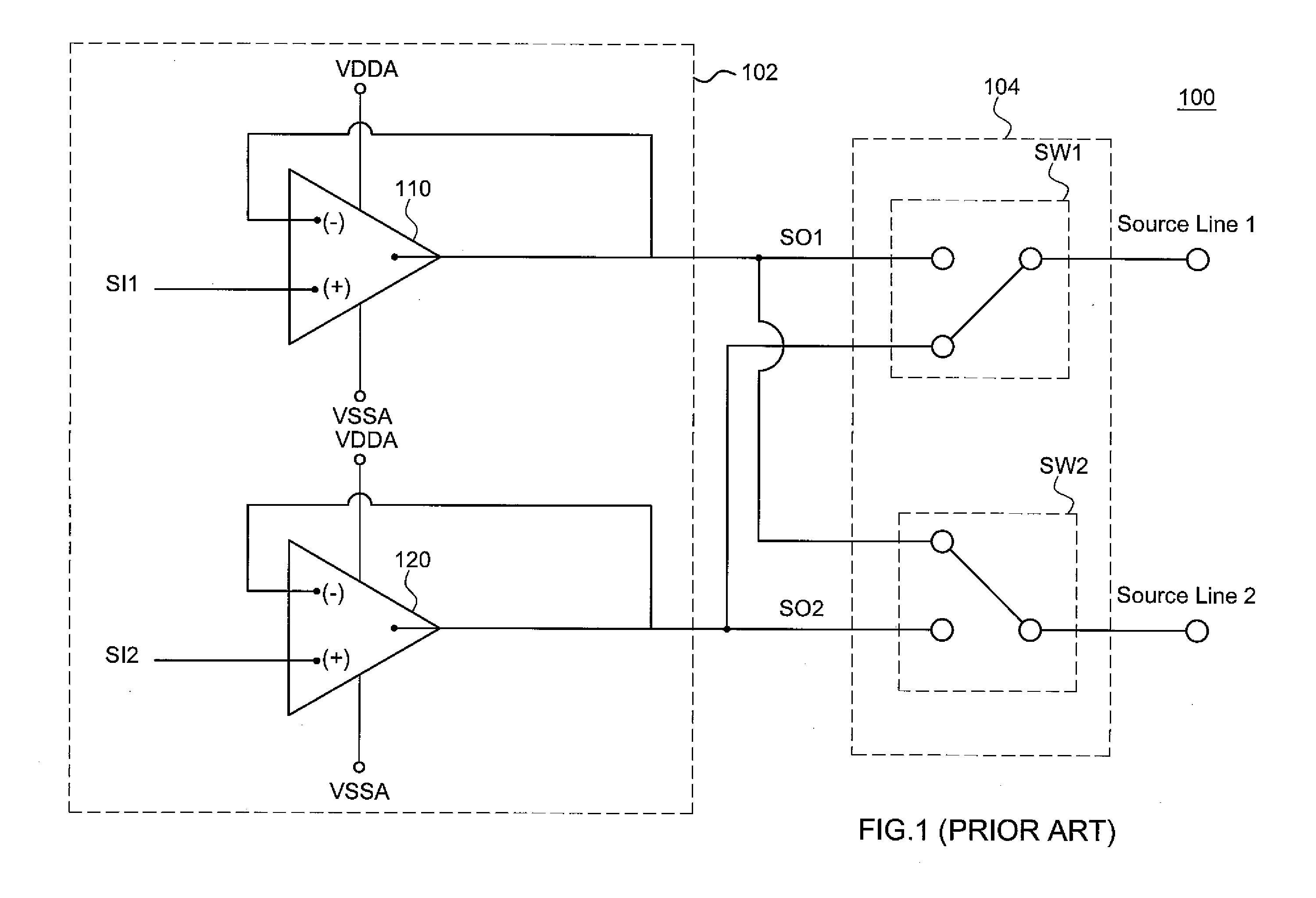
[0013]FIG. 1 is a schematic diagram of a conventional source driver device;

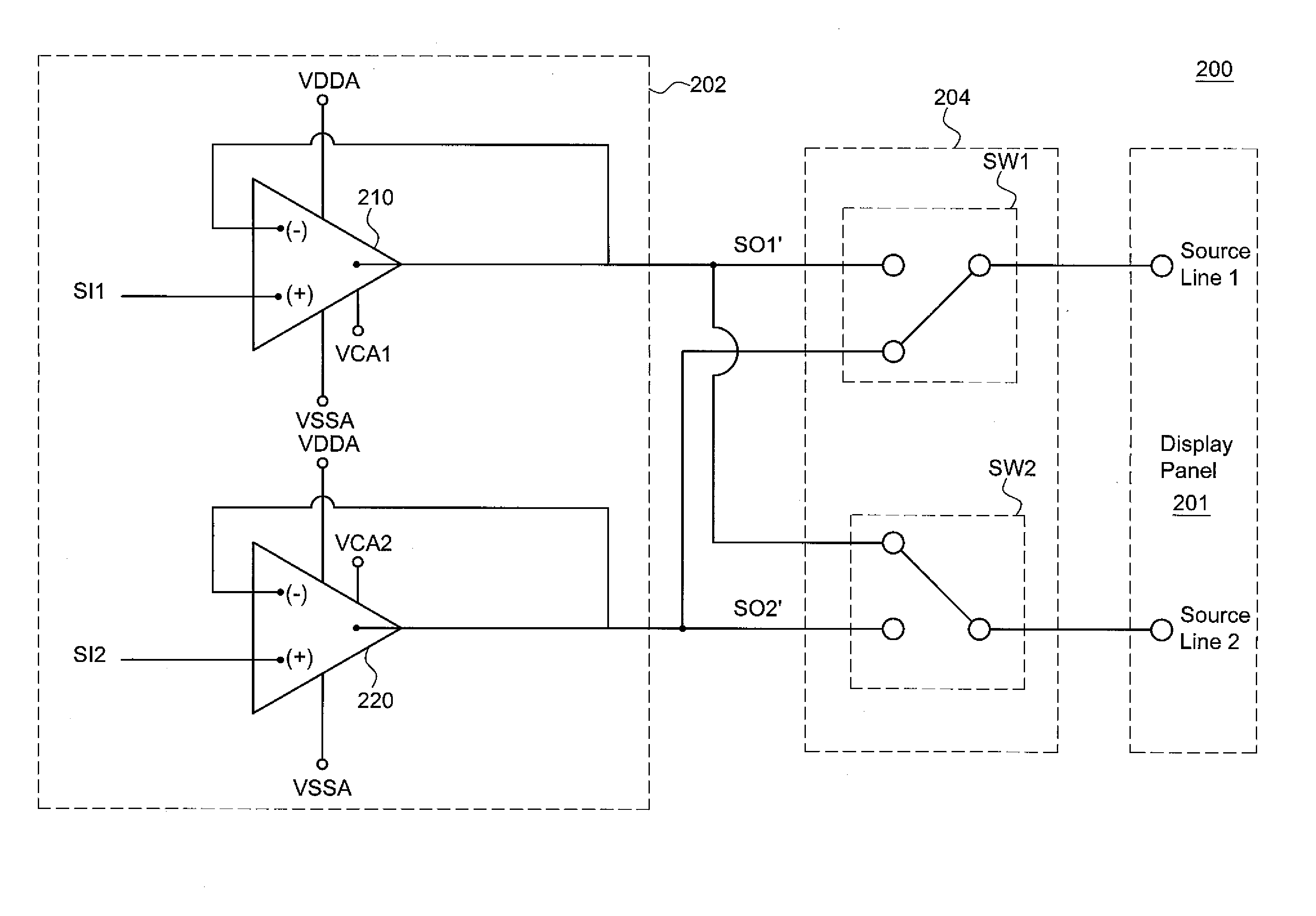
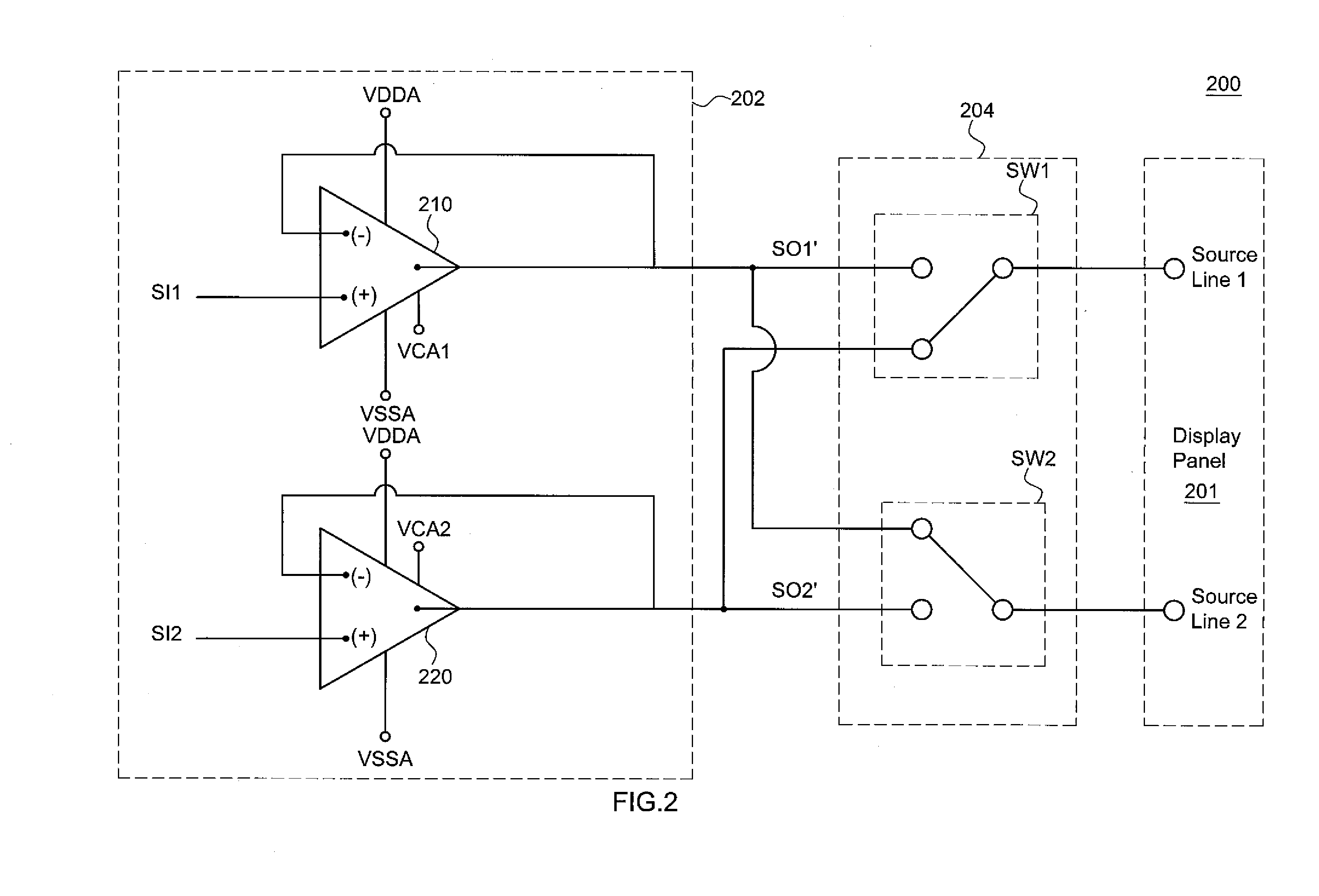
[0014]FIG. 2 is a schematic diagram of an exemplary source driver device according to one embodiment;

[0015]FIGS. 3A and 3B are more detailed schematic diagrams of first and second amplifier circuits of FIG. 2 in accordance with one embodiment;

[0016]FIGS. 4A and 4B are circuit diagrams of the first amplifier circuit of FIG. 3A and the second amplifier circuit of FIG. 3B in accordance with one embodiment, respectively;

[0017]FIGS. 5A and 5B are more detailed schematic diagrams of first and second amplifier circuits of FIG. 2 in accordance with another embodiment;

[0018]FIGS. 6A and 6B are circuit diagrams of the first amplifier circuit of FIG. 5A and the second amplifier circuit of FIG. 5B in accordance with one embodiment, respectively; and

[0019]FIG. 7 is a schematic block...


PUM


Abstract

A buffering circuit with reduced power consumption is provided. The output buffering circuit includes first and second amplifier circuits. The first amplifier circuit includes a first input stage and a first output stage both coupled between a first power voltage and a second power voltage lower than the first power voltage, and an assistant discharging unit configured to provide a discharging current flowing from a first output node to a first intermediate power voltage during a discharging operation of the first amplifier circuit. The second amplifier circuit includes a second input stage and a second output stage both coupled between the first power voltage and the second power voltage, and an assistant charging unit configured to provide a charging current flowing from a second intermediate power voltage to a second output node during a charging operation of the second amplifier circuit. The first and second amplifier circuits can have reduced output voltage ranges and hence reduced total power consumption.

Description

BACKGROUND[0001]1. Technical Field[0002]The embodiments described herein relate to a display device, and more particularly, to an output buffering circuit for a driver device, an amplifier circuit, and a display device employing the output buffering circuit.[0003]2. Description of the Related Art[0004]In general, a source driver chip for a display system includes several hundreds of source driving circuits, each for driving at least one source line of the panel in the display system. The power consumption of a single source driving circuit therefore has a large impact on the whole source driver chip. A source driving circuit generally includes an output buffer which takes a large part in the total power consumption and operating speed of the source driving circuit. For a portable electronic product, an output buffer that consumes less power can extend the life of the batteries. On the other hand, for applications of large-size LCDs (liquid crystal displays) that accompany relatively...

Claims


Application Information

Patent Timeline
Patent Type & Authority Applications(United States)
IPC IPC(8): G09G5/00H03F3/16H03L5/00
CPCG09G3/2092G09G2300/0426H03F3/3022G09G2360/18H03F1/0205G09G2330/021
Inventor WANG, JIA-HUITSAI, CHIEN-HUNGCHEN, YING-LIEHCHANG, CHIN-TIEN
Owner HIMAX TECH LTD
Why Eureka
Try Eureka