Wafer level camera module with molded housing and method of manufacturing

Active Publication Date: 2011-02-17
NANCHANG O FILM OPTICAL ELECTRONICS TECH CO LTD
View PDF123 Cites 49 Cited by
  • Summary
  • Abstract
  • Description
  • Claims
  • Application Information

AI Technical Summary

Benefits of technology

The present invention overcomes the problems associated with the prior art by providing a wafer level camera module capable of withstanding a solder reflow

Problems solved by technology

In manufacturing these camera modules, many problems are encountered by the camera module manufacturers.
As an example, bare ICD dies are extremely vulnerable to contamination when exposed to contaminants such as dust and/or other particulate debris.
Further, ICDs are extremely vulnerable when exposed to materials (e.g., adhesives) and processes (e.g., housing attachment, molding, lens attachment, etc.) used in the assembly of the camera modules.
Contamination typically results in the discarding of the defective image capture devices which can be extremely expensive, especially when yield losses are high.
Although the image capture devices of assembled camera modules are protected from contaminants outside of the camera module, they are still vulnerable to internal contaminants.
Such internal contaminants are usually the result of trapped dust, adhesives,

Method used


Image

  • Wafer level camera module with molded housing and method of manufacturing
  • Wafer level camera module with molded housing and method of manufacturing
  • Wafer level camera module with molded housing and method of manufacturing

Examples


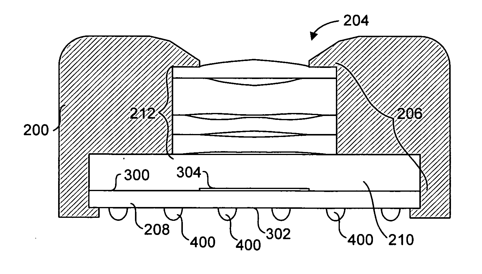
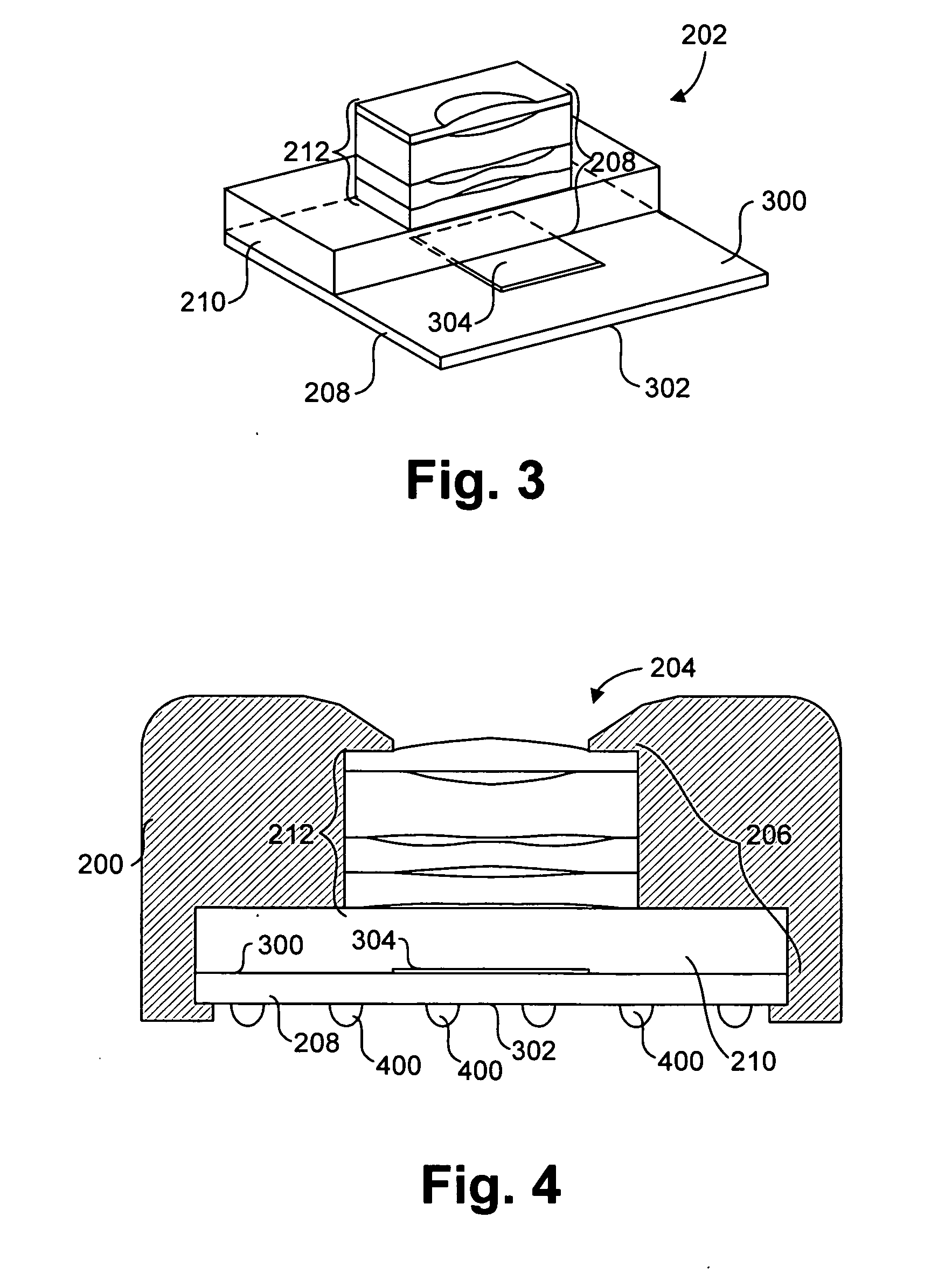
Embodiment Construction

The present invention overcomes the problems associated with the prior art, by providing a simplified wafer level camera module that can withstand reflow soldering conditions. In the following description, numerous specific details are set forth (e.g., number of lenses, type of epoxy, etc.) in order to provide a thorough understanding of the invention. Those skilled in the art will recognize, however, that the invention may be practiced apart from these specific details. In other instances, details of well known electronic assembly practices and equipment have been omitted, so as not to unnecessarily obscure the present invention.

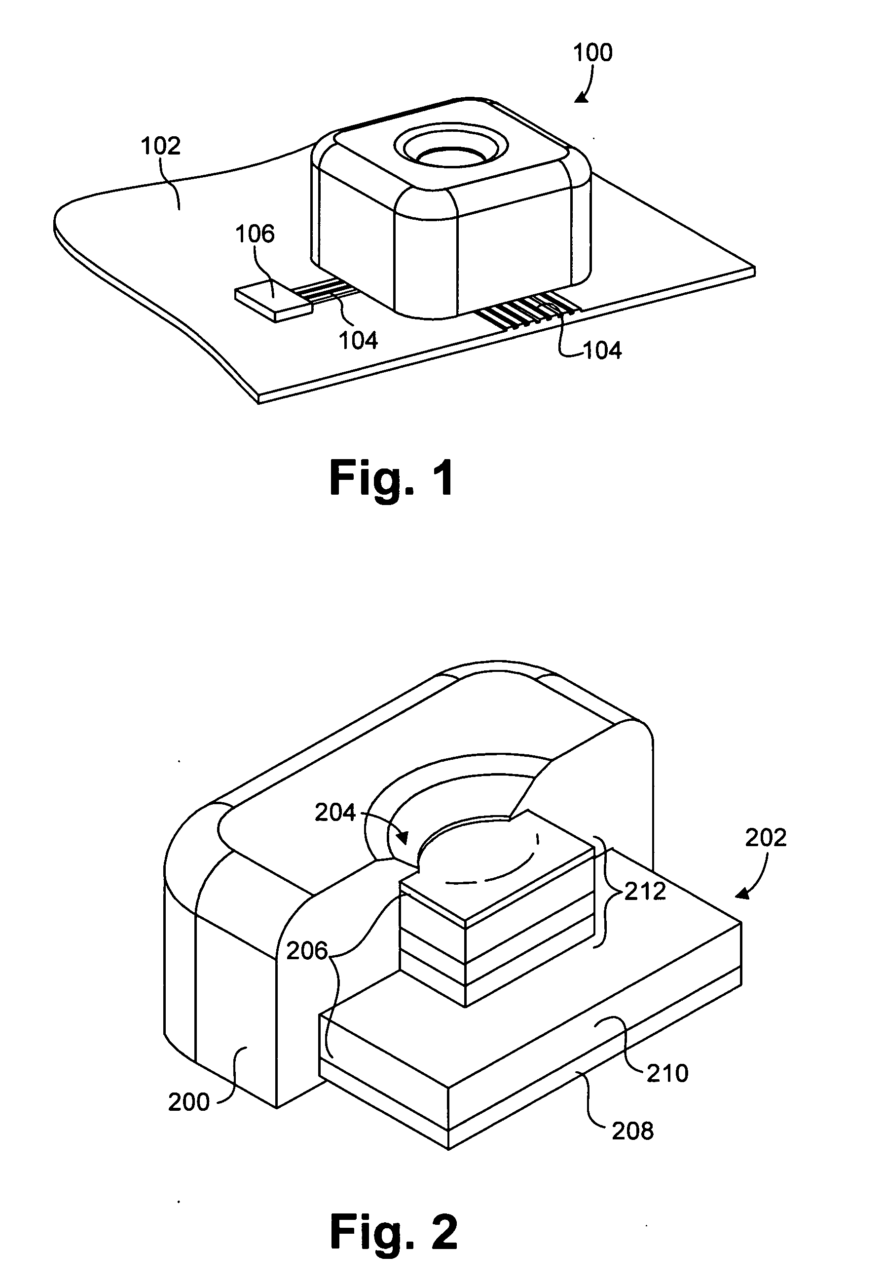
FIG. 1 is a perspective view of a camera module 100 according to one embodiment of the present invention. Camera module 100 is shown mounted on a portion of a printed circuit board (PCB) 102 that represents a main PCB of a camera hosting device (e.g., cell phone, PDA, etc.). Camera module 100 communicates electrically with other components of the hosting de...


PUM

PropertyMeasurementUnit
Transparencyaaaaaaaaaa

Abstract

A disclosed method of manufacturing a camera module includes providing an optical assembly, providing an integrated circuit image capture device (ICD), fixing the optical assembly directly to the ICD, then forming a housing directly over the optical assembly. The method further includes forming the housing over the ICD and the optical assembly via transfer molding. The method further includes forming solder balls on the rear surface of the ICD so as to enable the camera module to be reflow soldered to a host device. In an alternative embodiment of the present invention, the method includes providing a second ICD, providing a second optical assembly, providing a housing substrate, fixing the first optical assembly over the first ICD, fixing the second optical assembly over the second ICD, and forming the housing substrate over both the first and second optical assemblies. The alternative method further includes separating the housing substrate in to a first portion formed over the first optical assembly and second portion formed over the second optical assembly, providing a second housing substrate, and forming the second housing substrate over the first and second portions.

Description

BACKGROUND OF THE INVENTION1. Field of the InventionThis invention relates generally to electronic devices, and more particularly to digital camera modules. Even more particularly, this invention relates to a design for a simplified wafer level camera module that can be reflow soldered to a hosting device.2. Description of the Background ArtDigital camera modules are currently being incorporated into a variety of host devices. Such host devices include cellular telephones, personal data assistants (PDAs), computers, etc. Therefore, consumer demand for digital camera modules in host devices continues to grow.Host device manufacturers prefer digital camera modules to be small, so that they can be incorporated into the host device without increasing the overall size of the host device. Further, host device manufacturers prefer camera modules that minimally affect host device design. In meeting these requirements the host device manufacturers prefer camera modules that capture images of...

Claims


Application Information

Patent Timeline
IPC IPC(8): H04N5/225H01L31/18B23P19/04
CPCG02B13/0085H01L27/14618H01L27/14625Y10T29/49826H04N5/2257H05K3/3436H01L27/14685H01L2924/0002H04N23/57H01L2924/00H05K3/00H04N23/00
Inventor SINGH, HARPUNEETSHANGGUAN, DONGKAITAM, SAMUEL WAISING
Owner NANCHANG O FILM OPTICAL ELECTRONICS TECH CO LTD
Why Eureka
Try Eureka