

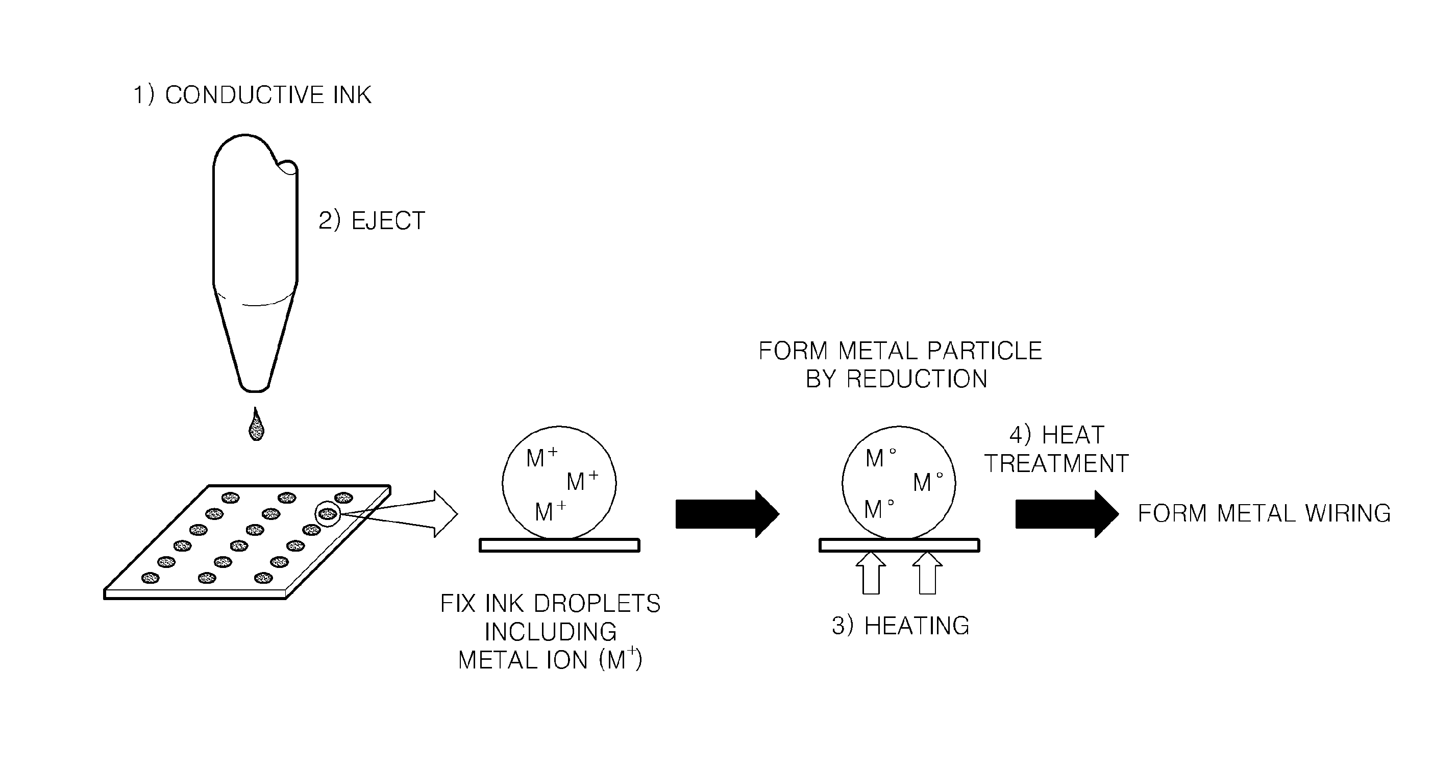
Conductive ink, method of preparing metal wiring using conductive ink, and printed circuit board prepared using method
a technology of conductive ink and metal wire, which is applied in the direction of inks, non-conductive materials with dispersed conductive materials, resistive material coatings, etc., can solve the problems of reducing the lifetime of conductive ink, clogging of the nozzle of the printing head, and difficulty in adjusting an amoun
- Summary
- Abstract
- Description
- Claims
- Application Information
AI Technical Summary
Benefits of technology
Problems solved by technology
Method used
Image

Examples
example 1
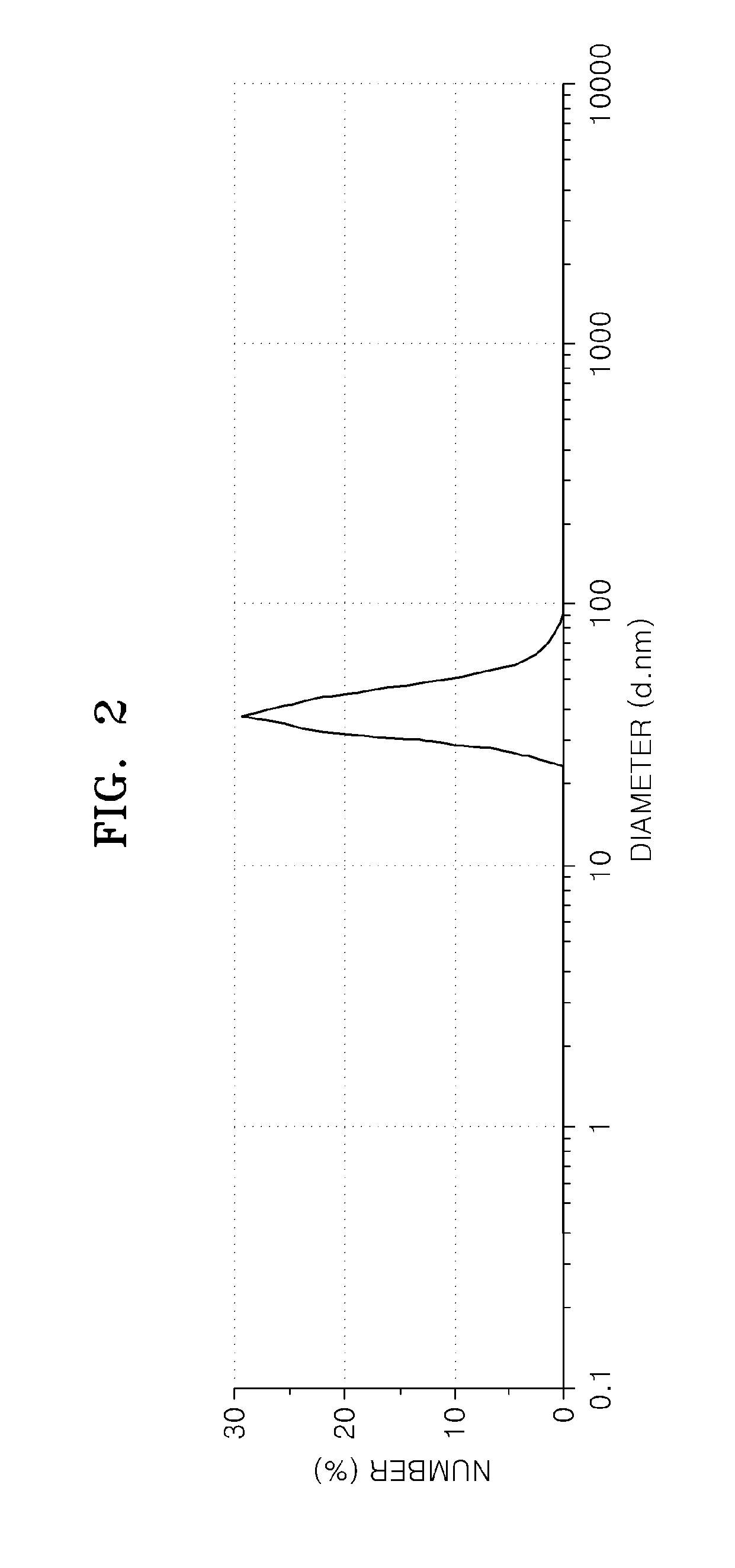
92.3 parts by weight of polyvinyl alcohol (molecular weight 10,000) and 61.5 parts by weight of AgNO3 were added to 100 parts by weight of polyethylene glycol #100. The resultant was stirred at room temperature, until the AgNO3 was completely dissolved, to prepare a conductive ink including metal ions. The conductive ink was printed on a glass substrate using an inkjet printer. The printed glass substrate was heated at a temperature of 75° C., to generate Ag nanoparticles. FIG. 2 shows an analysis of the grain sizes of the Ag nanoparticles. The Ag nanoparticles were heat-treated in a sintering furnace for three minutes, at a temperature of 150° C., to prepare micro-wiring.
example 2
A conductive ink was prepared in the same manner as in Example 1, except that polyethylene glyco #400 was substituted for the polyethylene glycol #100. The conductive ink was printed on a glass substrate using an inkjet printer. The printed glass substrate was heated at a temperature of 65° C., to generate Ag nanoparticles. Then, the glass substrate was heat-treated in a sintering furnace for 30 minutes, at a temperature of 150° C., to prepare micro-wiring.
As described above, according to the one or more of embodiments of the present disclosure, since a conductive ink includes metal ions, an unwanted increase in diameter and / or particle aggregation may be essentially prevented. Thus, the conductive ink may have a long storage life. By using the conductive ink, the nozzle of a print head may be prevented from clogging. Thus, the redispersion of metal nanoparticles and / or a filtering process for separating aggregated particles are not needed. Accordingly, material losses may be preven...
PUM
| Property | Measurement | Unit |
|---|---|---|
| Temperature | aaaaa | aaaaa |
| Temperature | aaaaa | aaaaa |
| Temperature | aaaaa | aaaaa |
Abstract
Description
Claims
Application Information