Light emitting apparatus

a technology of light emitting apparatus and light beam, which is applied in the direction of discharge tube/lamp details, lighting and heating apparatus, discharge tube luminescnet screens, etc., can solve problems such as reliability deterioration, achieve stable bonding force to the support material, prevent short-cutting between wiring patterns (electrode patterns on the support) and enhance light radiation efficiency and emission efficiency.

Active Publication Date: 2005-08-04
TOYODA GOSEI CO LTD
View PDF4 Cites 51 Cited by
  • Summary
  • Abstract
  • Description
  • Claims
  • Application Information

AI Technical Summary

Benefits of technology

[0042] In the light emitting apparatus of the invention, since the reflection layer is of a material that generates no intermetallic compound to a material of the conductive layer, no intermetallization is generated between the conductive layer and the reflection layer. Therefore, the light radiation efficiency and emission efficiency can be enhanced together.
[0043] Alternatively, since a barrier metal layer is formed between the conductive layer and the reflection layer and is of a material that prevents the generation of an intermetallic compound between the conductive layer and the reflection layer, the same effects can be obtained.
[0044] Alternatively, since the conductive layer comprises a barrier metal layer that prevents an aggregation in a material of the reflection layer, aggregation in the reflection layer material Ag alloy caused by a change in surrounding temperature or by the turning-on of LED element can be prevented, and therefore the stable bonding force to the support material can be obtained.
[0045] Alternatively, since the reflection layer is partially removed in accordance with the electrode of the LED element to expose a surface of the conductive layer, and the conductive layer is electrically connected through a bump material to the electrode of the LED element at the exposed surface, the bump material can be securely placed in the removed portion (indented portion) without flowing laterally due to temperature rise during the bump bonding process. Therefore, the short-cutting between wiring patterns (electrode patterns on the support) can be prevented.

Problems solved by technology

Such a residue causes deterioration in reliability such as short-circuiting.

Method used


Image

  • Light emitting apparatus
  • Light emitting apparatus
  • Light emitting apparatus

Examples


first embodiment

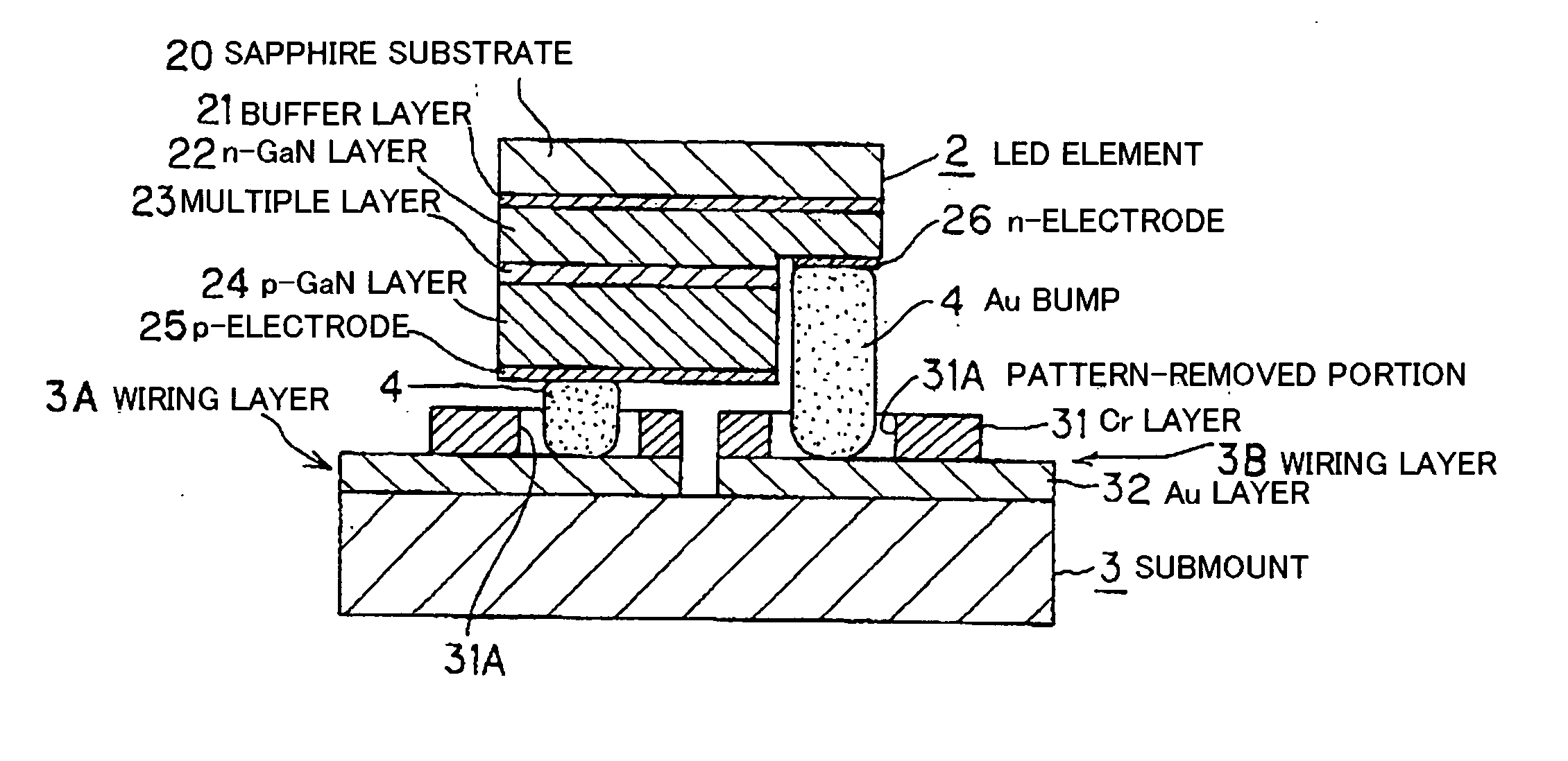
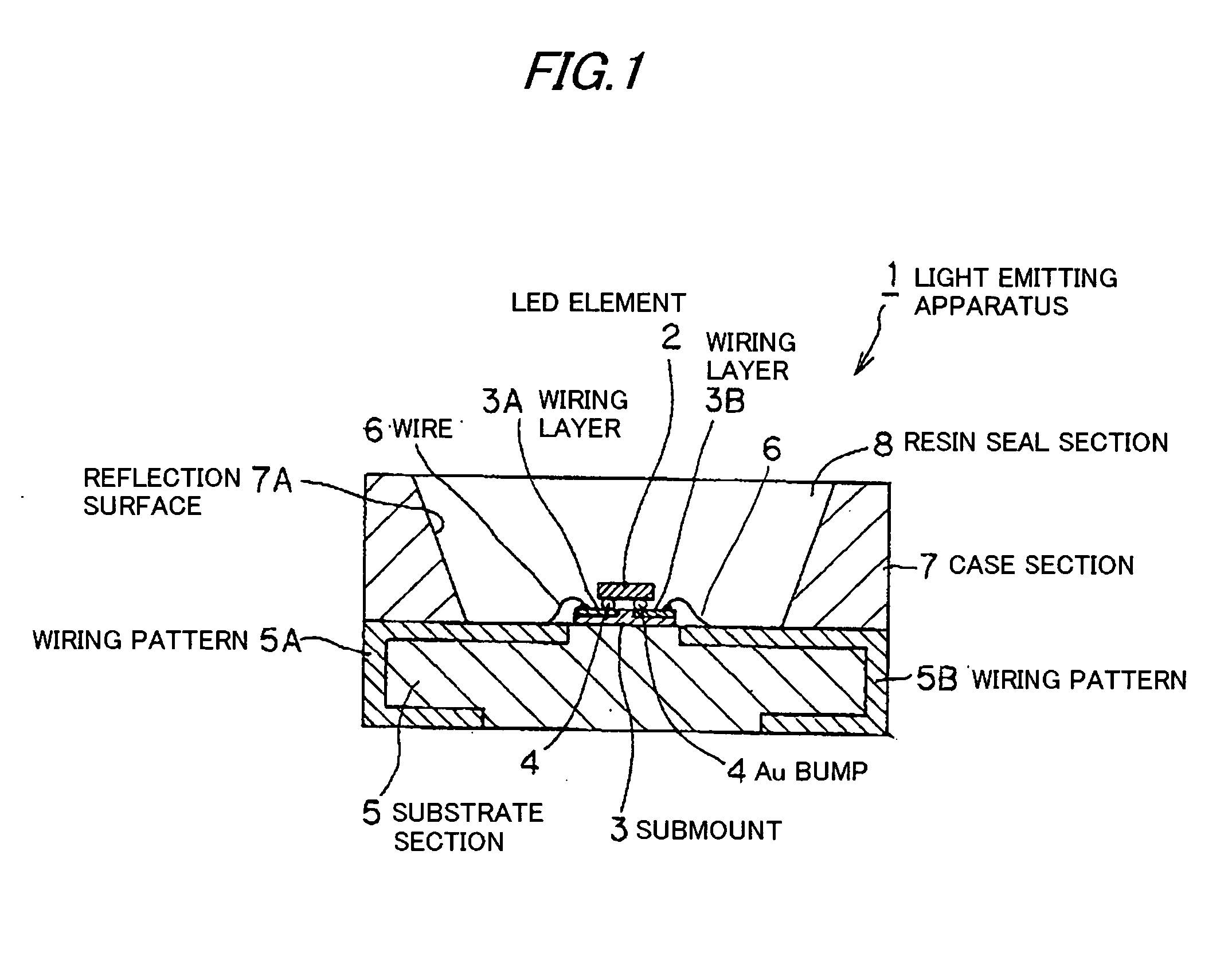
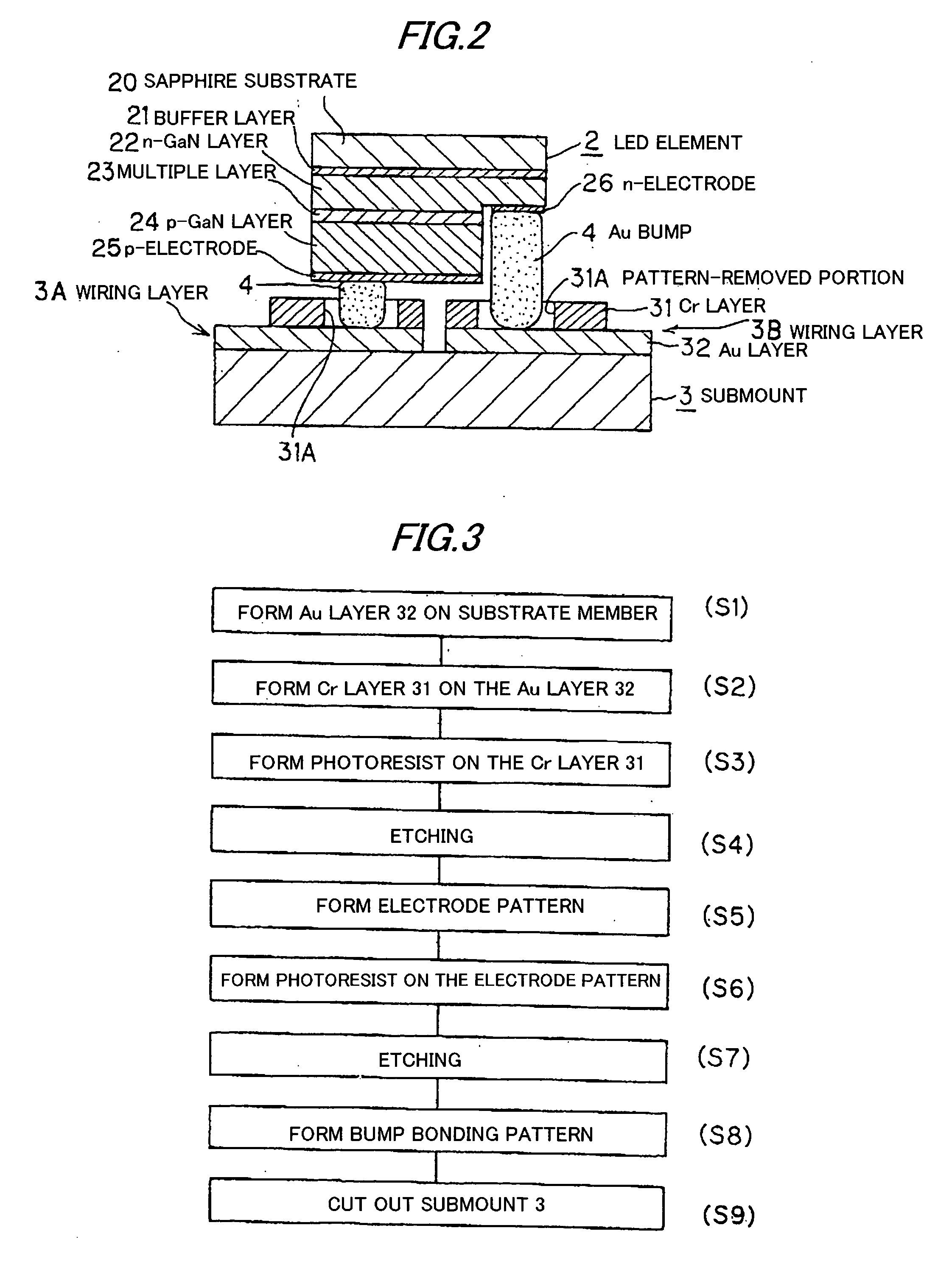
[0068] The process of fabricating the submount 3 of the first embodiment will be explained below referring to FIGS. 1, 2 and 3. FIG. 3 is a flowchart showing the process of fabricating the submount 3.

[0069] First, the Au layer 32 as the conductive layer is formed on the surface of the AlN substrate material by deposition (S1). Then, the Cr layer 31 is formed on the Au layer 32 by magnetron sputtering using a Cr target with Ar gas of 10−7 Torr (S2). Then, a photoresist is formed according to an electrode pattern on the Cr layer 31 (S3). Then, the Cr layer 31 is etched by a solution of cerium diammonium nitrate and perchloric acid and the Au layer 32 is further etched by nitrohydrochloric acid (S4). The electrode pattern is formed by the etching (S5). Then, a photoresist is formed according to the bonding pattern of Au bumps 4 on the Cr layer 31 (S6). Then, the Cr layer 31 is etched by the solution of cerium diammonium nitrate and perchloric acid (S7). By this etching, the pattern-rem...

second embodiment

[0083] The process of fabricating the submount 3 of the second embodiment will be explained below referring to FIGS. 4 and 5. FIG. 5 is a flowchart showing the process of fabricating the submount 3.

[0084] First, the Au layer 32 as the conductive layer is formed on the surface of the AlN substrate material by deposition (S1). Then, the barrier metal layer 33 of chromium oxide is formed on the Au layer 32 by magnetron sputtering using a Cr target with Ar / N2 / O2 mixed gas of 10−7 Torr (S2). Then, the Al layer 34 is formed on the barrier metal layer 33 by deposition (S3). Then, a photoresist is formed according to an electrode pattern on the Al layer 34 (S4). Then, the Al layer 34 is etched by a solution of sodium hydroxide, the barrier metal layer 33 is etched by cerium diammonium nitrate and perchloric acid, and the Au layer 32 is etched by nitrohydrochloric acid (S5). The electrode pattern is formed by the etching (S6). Then, a photoresist is formed according to the bonding pattern of...

third embodiment

[0093] The process of fabricating the submount 3 of the third embodiment will be explained below referring to FIGS. 6 and 7. FIG. 7 is a flowchart showing the process of fabricating the submount 3.

[0094] First, the Au layer 32 as the conductive layer is formed on the surface of the AlN substrate material by deposition (S1). Then, the Ag alloy layer 36 is formed on the Au layer 32 by magnetron sputtering using an Ag alloy target with Ar gas of 10−7 Torr (S2). Then, a photoresist is formed according to an electrode pattern on the Ag alloy layer 36 (S3). Then, the Ag alloy layer 36 is etched by a solution of chromic anhydride, perchloric acid and concentrated sulfuric acid and the Au layer 32 is further etched by nitrohydrochloric acid (S4). The electrode pattern is formed by the etching (S5). Then, a photoresist is formed according to the bonding pattern of Au bumps 4 on the Ag alloy layer 36 (S6). Then, the Ag alloy layer 36 is etched by the solution of chromic anhydride, perchloric ...


PUM


Abstract

A light emitting apparatus has: a support; a wiring layer that is formed on the support; and an LED element that is flip-chip mounted on the wiring layer formed on the support. The wiring layer has: a conductive layer that is formed on the support and is electrically connected to an electrode of the LED element; and a reflection layer that is formed on the conductive layer that has a light reflection property to allow a radiated light from the LED element to be reflected thereon. The reflection layer is of a material that generates no intermetallic compound to a material of the conductive layer.

Description

[0001] The present application is based on Japanese patent application No. 2004-006037, the entire contents of which are incorporated herein by reference. BACKGROUND OF THE INVENTION [0002] 1. Field of the Invention [0003] This invention relates to a light emitting apparatus and, particularly, to a flip-chip type light emitting apparatus that allows light radiated in the direction of an electrode-forming surface of LED element to be effectively used. [0004] 2. Description of the Related Art [0005] Light emitting apparatuses are conventionally known that have an LED (light emitting diode) element being flip-chip mounted (herein called flip-chip type) and that use mainly light radiated in the direction of a transparent substrate, such as a sapphire, of the LED element. [0006] Further, in order to enhance the light radiation efficiency, a flip-chip type light emitting apparatus (prior art 1) is known that is composed of: a support for mounting an LED element thereon; a conductive wirin...

Claims


Application Information

Patent Timeline
Patent Type & Authority Applications(United States)
IPC IPC(8): F21V7/00H01J1/62H01L33/32H01L33/60H01L33/62
CPCH01L33/405H01L2224/16H01L2224/48091H01L2924/00014
Inventor HIROSE, MINORU
Owner TOYODA GOSEI CO LTD
Why Eureka
Try Eureka