Three-dimensional conductive patterns and inks for making same

a three-dimensional, conductive pattern technology, applied in the field of polymerizable conductive ink formulations, can solve the problems of low resistivity, high aspect ratio of printed patterns, flow of ink on the substrate, etc., and achieve the effect of increasing the conductivity of printed patterns, high aspect ratio, and easy customization

Inactive Publication Date: 2015-12-17
YISSUM RES DEV CO OF THE HEBREWUNIVERSITY OF JERUSALEM LTD
View PDF5 Cites 50 Cited by
  • Summary
  • Abstract
  • Description
  • Claims
  • Application Information

AI Technical Summary

Benefits of technology

[0117]In some embodiments, the nanoparticles or microparticles may be stabilized in the formulation by one or more stabilizers (dispersing agents, dispersants) to prevent aggregation and / or agglomeration of the nanoparticles and to enable a stable dispersion. Such materials may be selected amongst surfactants and / or polymers. The stabilizer may have ionic or non-ionic functional groups, or a block co-polymer containing both. It may also be a volatile stabilizer which evaporates during the curing process; thus enabling higher conductivities after the decomposition and sintering of the pattern.
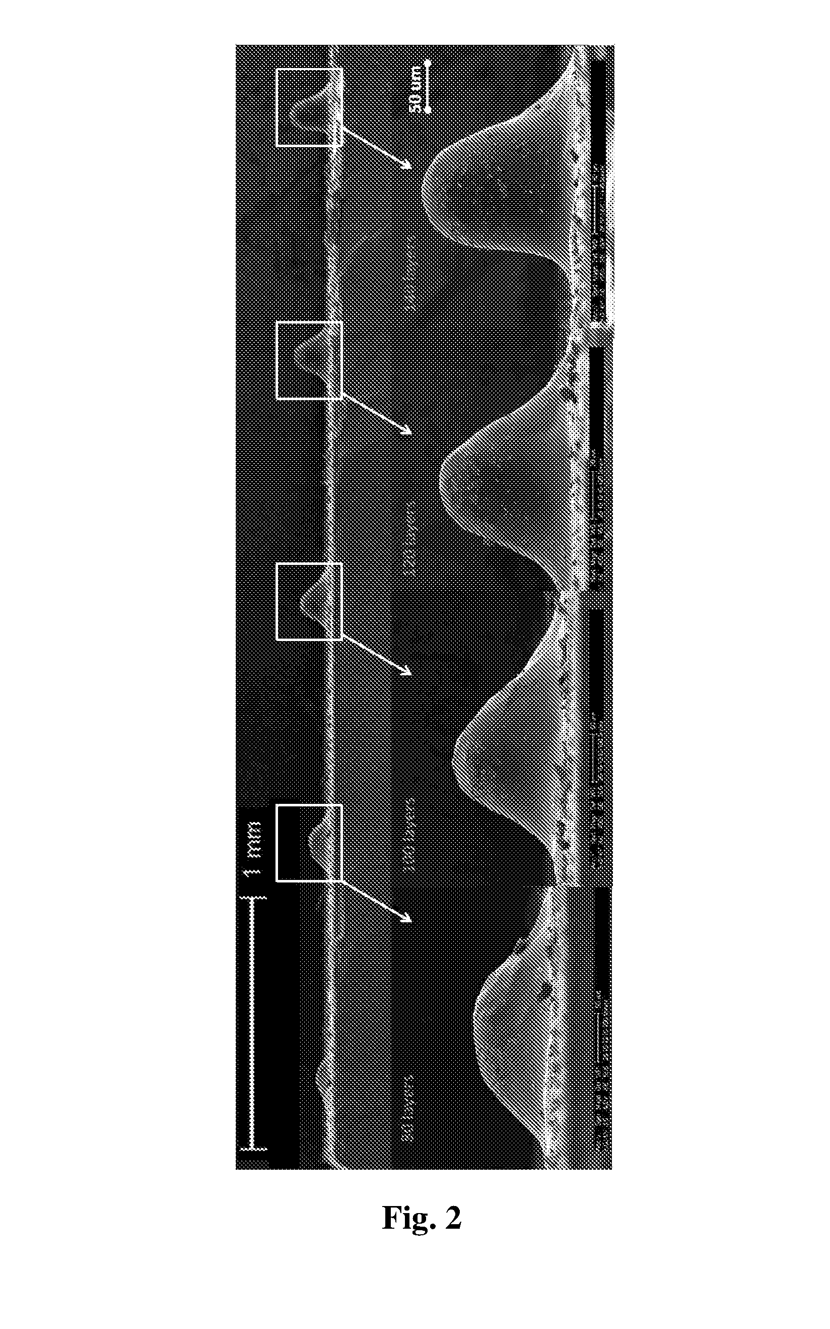
[0122]The conductive pattern obtained by the method of the invention is achieved by printing multiple layers of ink formulation, followed by performing on each layer immediately after it is printed, a curing process, and then optionally a sintering process on one or more layers in order to increase the conductivity of the pattern. Along with an increase in the number of layers, the vertical wall height increases substantially, whereas the horizontal width remains narrow, and thereby, obtaining a structure of high aspect ratio.
[0123]As the process of the invention permits layering of an infinite number of ink layers (repetitions of step (a) in the above process) on a surface region, the resulting pattern with a defined aspect ratio and conductivity or the size and dimensions of the final printed object may be easily tailored. As a person versed in the art would additionally understand, the process of the invention requires curing to be carried out on only a portion of the monomers / oligomers in the formed pattern, thus allowing nanoparticles or microparticles sintering to reach completion. Following the sintering of the last material layer, the pattern may be thermally treated or washed in order to remove the unreacted monomers and / or oligomers and further remove the polymerized material, leaving behind the sintered pattern decorated by material voids (previously occupied by the unreacted monomers and / or oligomers and the polymerized material). These voids may be further filled with metal source which converts into continuous metallic 3D structure.
[0125]The conductive pattern or object formed by any one process of the invention, is characterized by high aspect ratio (thus rendering it 3D) and high conductivity. The aspect ratio of a pattern defines a ratio of the height of pattern to its width. A printed pattern with a high aspect ratio is characterized by a long vertical axis and a short horizontal width.

Problems solved by technology

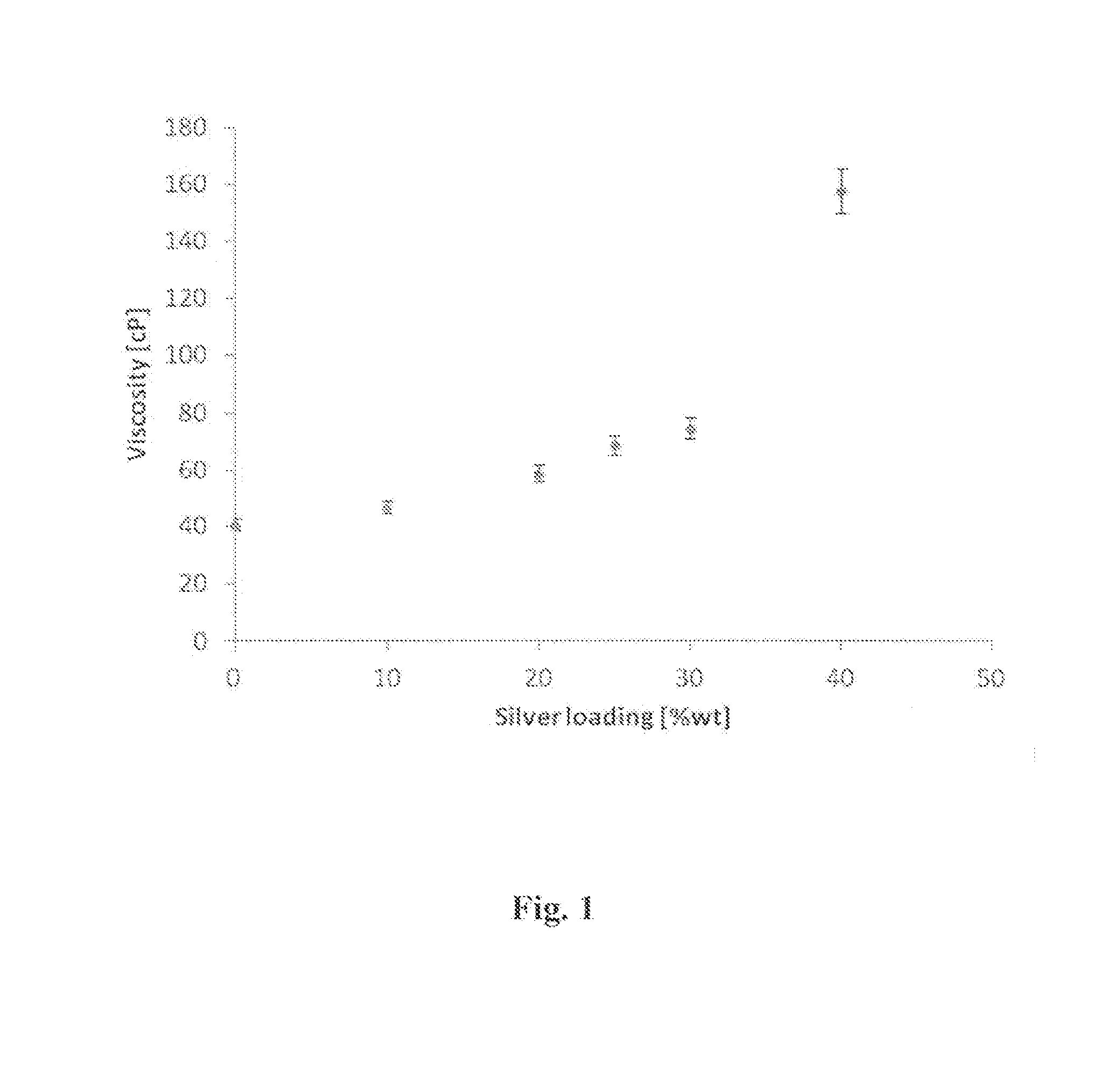
One of the obstacles towards achieving high aspect ratio of the printed pattern is the flow of the ink on the substrate due to inappropriate ink viscosity and surface tension.
This very low resistivity was due to the presence of the polymeric matrix of the ink after UV exposure.

Method used


Image

  • Three-dimensional conductive patterns and inks for making same
  • Three-dimensional conductive patterns and inks for making same
  • Three-dimensional conductive patterns and inks for making same

Examples


example 1

I. Example 1

Obtaining Film from Oil-in-Water (O / W) Emulsion

[0182]In preliminary experiments, the polymerization of the emulsion was tested by exposing a milliliter droplet to a curing source to a period of time sufficient to transform the polymerizable monomer into a solid polymer form.

[0183]Oil-in-water (O / W) emulsion was prepared by homogenizing the monomers in water while using Tween 80 as an emulsifier to obtain the emulsion which the droplet was taken from. The droplet was then exposed to UV light for a few seconds. The liquid droplet immediately transformed into solid, indicating that in spite of the high turbidity, the composition of the emulsion enabled polymerization.

Silver Nanoparticles Preparation:

[0184]The synthesis of silver NP dispersion (42% wt) was performed as described by Magdassi et al. [12], yielding nanoparticles which are stabilized by polyacrylic acid sodium salt (PAA, MW 8 kD) having an average size of 14±3 nm and zeta potential of −42 mV. The resulting dispe...

example 2

II. Example 2

3D Printing Pattern of Dots on Substrate

Materials and Methods of Preparation

UV Reactive Oil Phase Preparation:

[0191]The oil phase was composed of the following components:

[0192](1) Monomers: Dipentaerythnitol Hexaacrylate (DPHA) and Trimethylolpropane Triacrylate (TMPTA) at 2:3 weight ratio.

[0193](2) a mixture of photoinitators: Ethyl-4-dimethylaminobezoate (EDMAB) 32%, 2-Isopropylthioxanthon 13%, 2-benzyl-2 dimethylamoni-1-94-morpholinophenyl)-butanone-1 12%, dimethyl-1,2-diphenyllehan-1-one 28%, and Benzophenon 15%, all dissolved at a 1:2 weight ratio with Dipropylenglycol Diacrylate (DPGDA).

[0194]Then the two solutions of monomers and photoinitiators were mixed at a 1:1 weight ratio. The obtained oil phase was a clear solution with a yellowish color.

Aqueous Dispersion of Nanoparticles Preparation:

[0195]The silver NPs were prepared similarly as described above in Example 1. A 30 wt % silver dispersion was prepared by mixing the silver powder in triple-distilled water ...

example 3

III. Example 3

3D Printing Pattern of Lines on Substrate

Materials and Methods of Preparation

Oil-in-Water Emulsion Preparation:

[0209]The composition of the ink formulation was similar to that described in Example 2.

[0210]In general, the same behavior was observed for ink-jet-printed lines which were dipped into NaCl solution as observed for the printed dots of Example 2. FIG. 6 shows how the resistance of the printed lines decreases with the increase in the number of printed layers (and subsequent increase in metal content) until it reaches a minimum of about 120 ohms. Without being bound by theory, since the resistance measurement was performed by contacting the multimeter probes on top of the printed line, it could be that the upper layer was composed of a polymer, which is an insulator, above the nanoparticles, leading to resistance lower than the actual situation. Therefore, the ink was printed on top of two copper electrodes and the resistance between them was measured. For a pri...


PUM

PropertyMeasurementUnit
aspect ratioaaaaaaaaaa
time periodaaaaaaaaaa
timeaaaaaaaaaa

Abstract

The invention generally relates to polymerizable conductive ink formulations comprising at least one metal source, at least one monomer and / or oligomer and a polymerization initiator, and uses thereof for printing three-dimensional functional structures. In particular a method of fabricating a three-dimensional conductive pattern on a substrate is disclosed, the method comprising: a) forming a pattern on a surface region of a substrate by using an ink comprising at least one metal source, at least one liquid polymerizable monomer and / or oligomer, and at least one polymerization initiator; b) polymerizing at least a portion of said liquid monomer and / or oligomer; c) rendering the metal source a continuous percolation path for electrical conductivity (sintering); d) repeating steps (a), (b) and optionally (c) to obtain a three-dimensional conductive pattern.

Description

TECHNOLOGICAL FIELD[0001]The invention generally relates to polymerizable conductive ink formulations and uses thereof for printing three-dimensional functional structures.BACKGROUND OF THE INVENTION[0002]Digital printing, typically known as digital fabrication, enables fabrication of various functional coatings and devices, and provides the ability to create three-dimensional (3D) structures and patterns with high aspect ratios.[0003]Digital printing is known in the art to afford functional coatings of electrodes for devices, such as sensors and electroluminescent devices. Sriprachuabwong et al. [1] describes printed polyaniline electrodes as ascorbic acid sensors and Azouble et al. [2] describes printed carbon nanotubes as electrodes for electroluminescent devices.[0004]Printed electronics mainly focuses on conducting patterns which are formed by printing nanoparticles and precursors; among these, the most common are silver inks which are mainly used for the fabrication of simple ...

Claims


Application Information

Patent Timeline
Patent Type & Authority Applications(United States)
IPC IPC(8): H05K3/12H05K1/02B29C67/00B22F1/0545
CPCH05K3/125B29C67/0059B29C67/0066H05K1/0296H05K2201/09218B29K2995/0005B33Y10/00B33Y80/00B29K2105/0002C09D11/52H01B1/22H05K1/097H05K3/1283H05K3/245H05K2203/1131H05K2203/1157H05K2203/1476C09D11/101B29C64/112B29C64/135Y02P10/25B22F1/0545B22F10/14B22F10/12B33Y70/10
Inventor MAGDASSI, SHLOMOSHAPIRA, AMIRLAYANI, MICHAELCOOPERSTEIN, IDO
Owner YISSUM RES DEV CO OF THE HEBREWUNIVERSITY OF JERUSALEM LTD
Why Eureka
Try Eureka