

Conductive particles and method and device for manufacturing the same, anisotropic conductive adhesive and conductive connection structure, and electronic circuit components and method of manufacturing the same
a technology of anisotropic conductive adhesive and conductive connection structure, which is applied in the direction of non-conductive materials with dispersed conductive materials, natural mineral layered products, synthetic resin layered products, etc., can solve the problems of particle flow out, particle overflow, and irregular plating layer,
- Summary
- Abstract
- Description
- Claims
- Application Information
AI Technical Summary
Benefits of technology
Problems solved by technology
Method used
Image

Examples
example 1
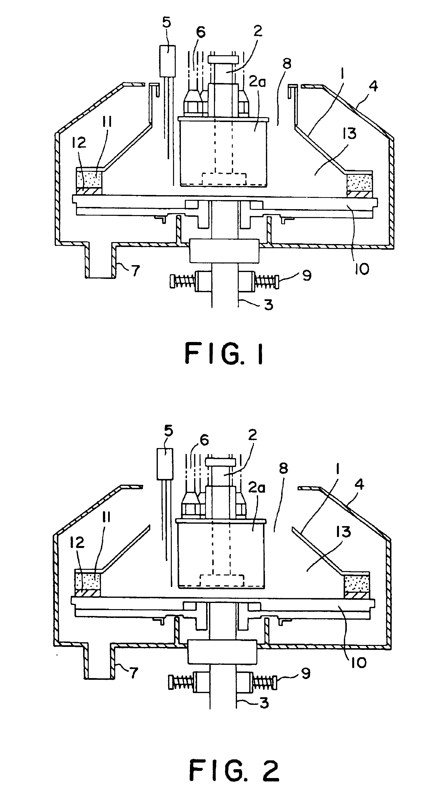
[0431]A nickel plating layer is formed as a conductive base layer on each of organic resin fine particles obtained by copolymerizing styrene and divinylbenzene; thus, a nickel plating fine particle having an average particle size of 75.72 μm and a standard deviation of 2.87 μm was obtained. The resulting nickel plating fine particles (16 g) were subjected to nickel plating on their surface by using a manufacturing device for conductive fine particles shown in FIG. 1.
[0432]With respect to the porous member 12, a porous member having a pore size of 20 μm, formed by high-density polyethylene, was used. Metal nickel was used as the anode 2a.
[0433]A Watt bath was used as the plating solution. The composition of the applied Watt bath had a nickel concentration of 42 g / L, nickel sulfate 150 g / L, and boric acid 31 g / L.
[0434]Power was applied across the electrodes with a voltage of 14 to 15 V for 25 minutes, under the conditions that the temperature of the plating solution was 5° C., the cu...
example 3
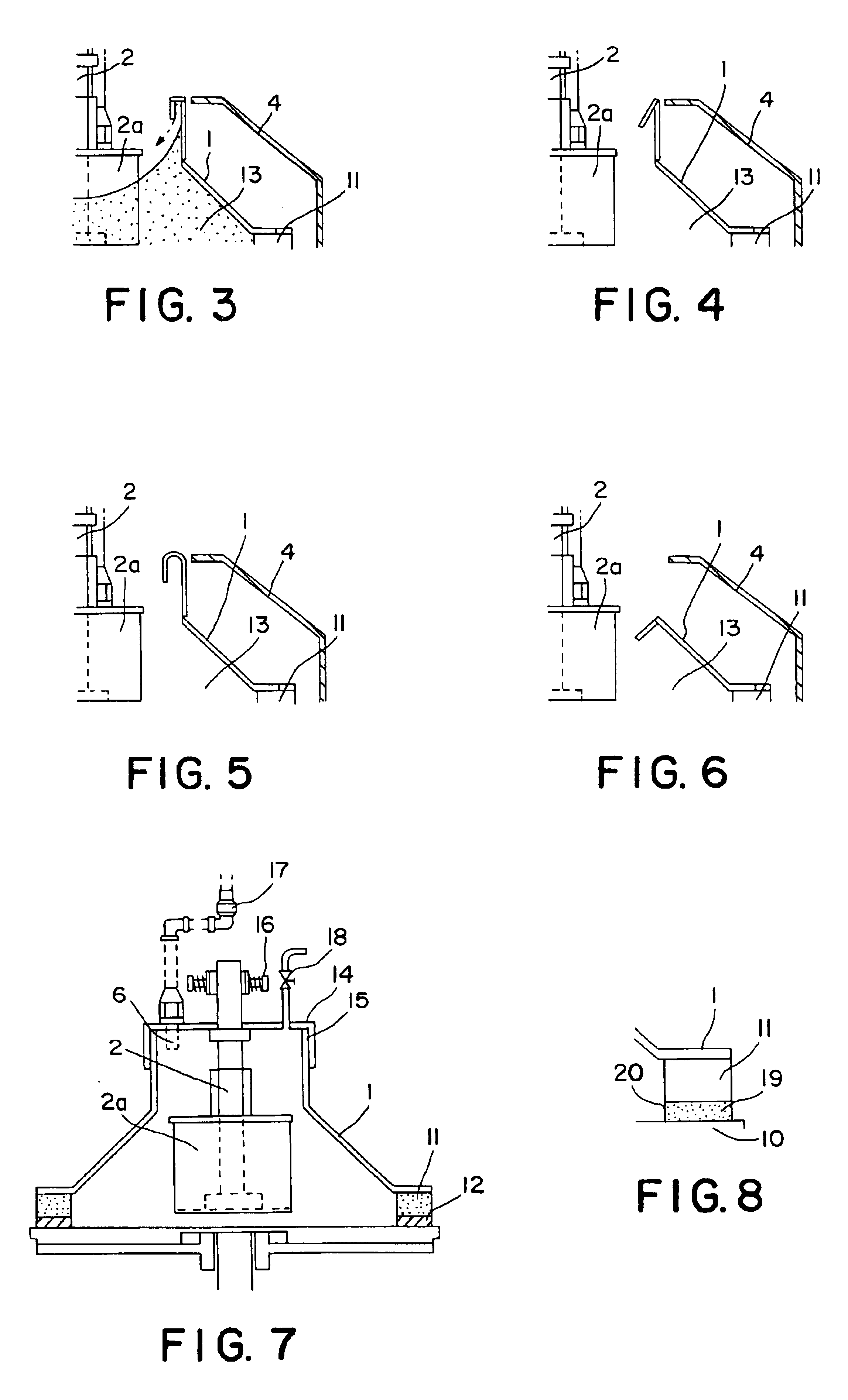
[0442]Plating was carried out in the same manner as Example 1 except that a manufacturing device for conductive fine particles shown in FIG. 1 was used as the manufacturing device for conductive fine particles, and that as illustrated in FIG. 8, a porous member, which was formed by affixing a nylon filter having a pore size of 10 μm onto the inner side surface on the treatment chamber side of a porous member having a pore size of 70 μm made from polypropylene, was used as a porous member 12.
[0443]During the rotation of the treatment chamber, the plating solution, which was subjected to a force in the outer circumferential direction due to the effect of a centrifugal force, formed a vortex having a mortar-like shape; however, there was no overflowing from the upper opening of the hollow cover 1.
[0444]The nickel plated resin fine particles having a nickel plated layer as the outermost layer thus obtained were observed under a microscope, and all the particles existed as individually i...
example 4
[0446]A nickel plating layer was formed as a conductive base layer on each of organic resin fine particles obtained by copolymerizing styrene and divinylbenzene; thus, a nickel plating fine particle having an average particle size of 250.68 μm and a standard deviation of 8.02 μm was obtained. The resulting nickel plating fine particles (30 g) were subjected to nickel plating on their surface by using a manufacturing device for conductive fine particles shown in FIG. 1.
[0447]With respect to the porous member 12, a porous member having a pore size of 70 μm, formed from polypropylene, was used. Metal nickel was used as the anode 2a. A Watt bath was used as the plating solution.
[0448]Power was applied across the electrodes with a voltage of 16 to 17 V for 20 minutes, under the conditions that the temperature of the plating solution was 50° C., the current was 38 A, and the current density was 0.65 A / dm2. The peripheral velocity of the treatment chamber was set at 250 m / min, and the rota...
PUM
| Property | Measurement | Unit |
|---|---|---|
| melting point | aaaaa | aaaaa |
| thickness | aaaaa | aaaaa |
| thermal conductivity | aaaaa | aaaaa |
Abstract
Description
Claims
Application Information