Structure for protecting an integrated circuit against electrostatic discharges

a technology for integrated circuits and structures, applied in emergency protective arrangements for limiting excess voltage/current, electrical equipment, transistors, etc., can solve problems such as destroying circuit elements, affecting circuit operation, and affecting circuit operation

Inactive Publication Date: 2011-02-24
STMICROELECTRONICS SRL
View PDF7 Cites 21 Cited by
  • Summary
  • Abstract
  • Description
  • Claims
  • Application Information

AI Technical Summary

Benefits of technology

[0022]Thus, an object of an embodiment of the present invention is to provide a structure of protection against electrostatic discharges which overcomes all or part of the disadvantages of conventional protection structures.

Problems solved by technology

Such a circuit generally receives and / or provides signals of low voltage level (for example, from 0.6 to 3 V) and low current intensity (for example, from 1 μA to 10 mA), and is likely to be damaged in the occurrence of overvoltages or overcurrents between terminals of the package.
Such overvoltages may reach several thousands of volts and destroy elements of the circuit.
A disadvantage of such a protection structure lies in the fact that diodes 12 and 13 have significant stray capacitances.

Method used


Image

  • Structure for protecting an integrated circuit against electrostatic discharges
  • Structure for protecting an integrated circuit against electrostatic discharges
  • Structure for protecting an integrated circuit against electrostatic discharges

Examples


Embodiment Construction

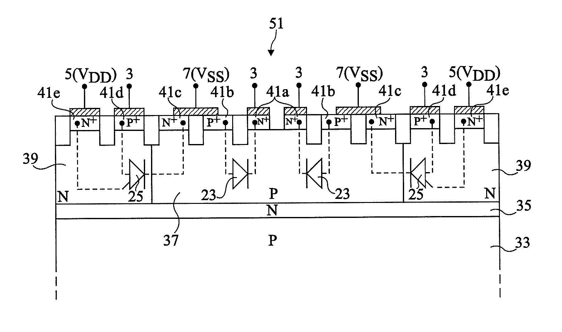
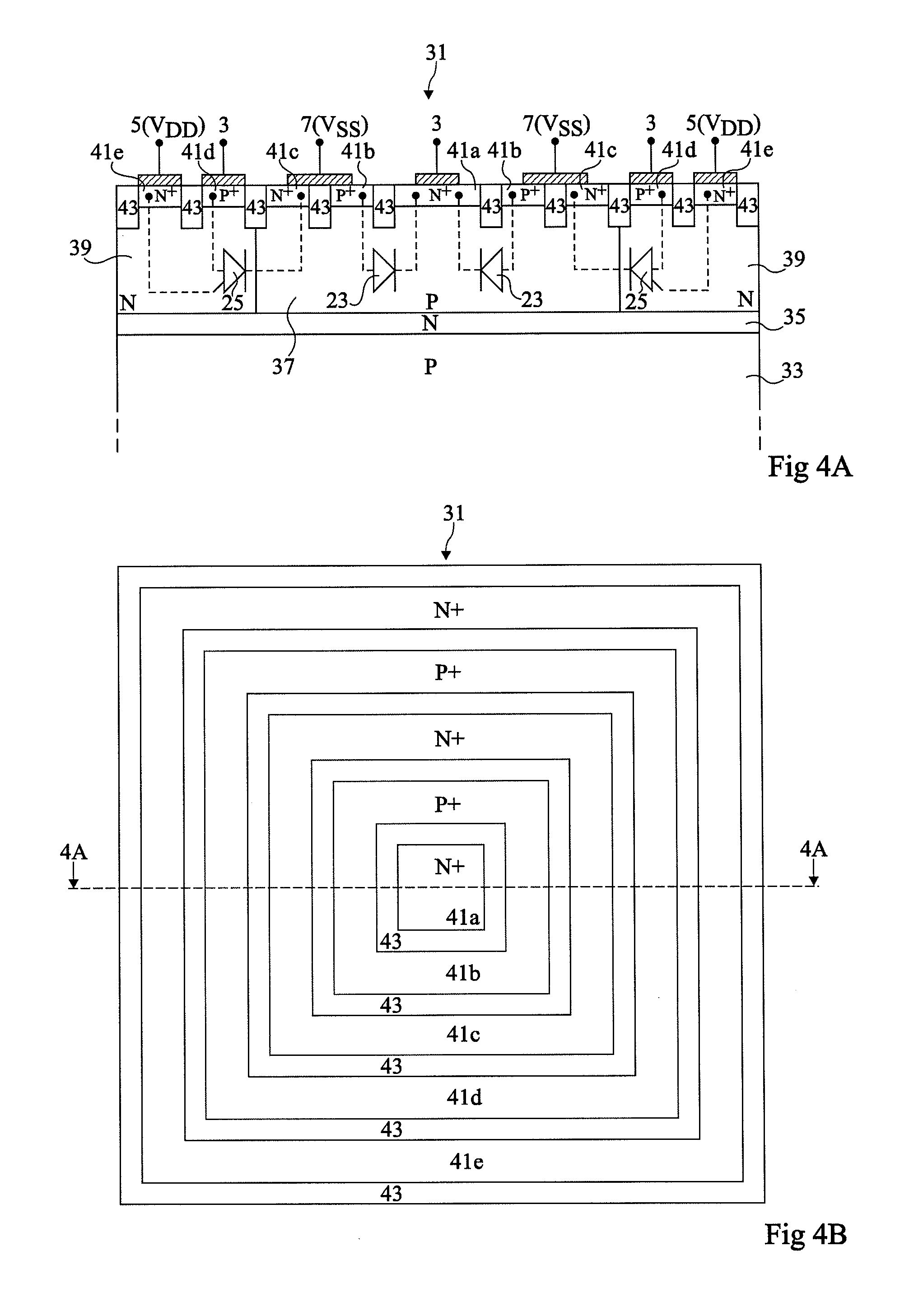
[0045]For clarity, the same elements have been designated with the same reference numerals in the different drawings and, further, as usual in the representation of integrated circuits, the various drawings are not to scale.

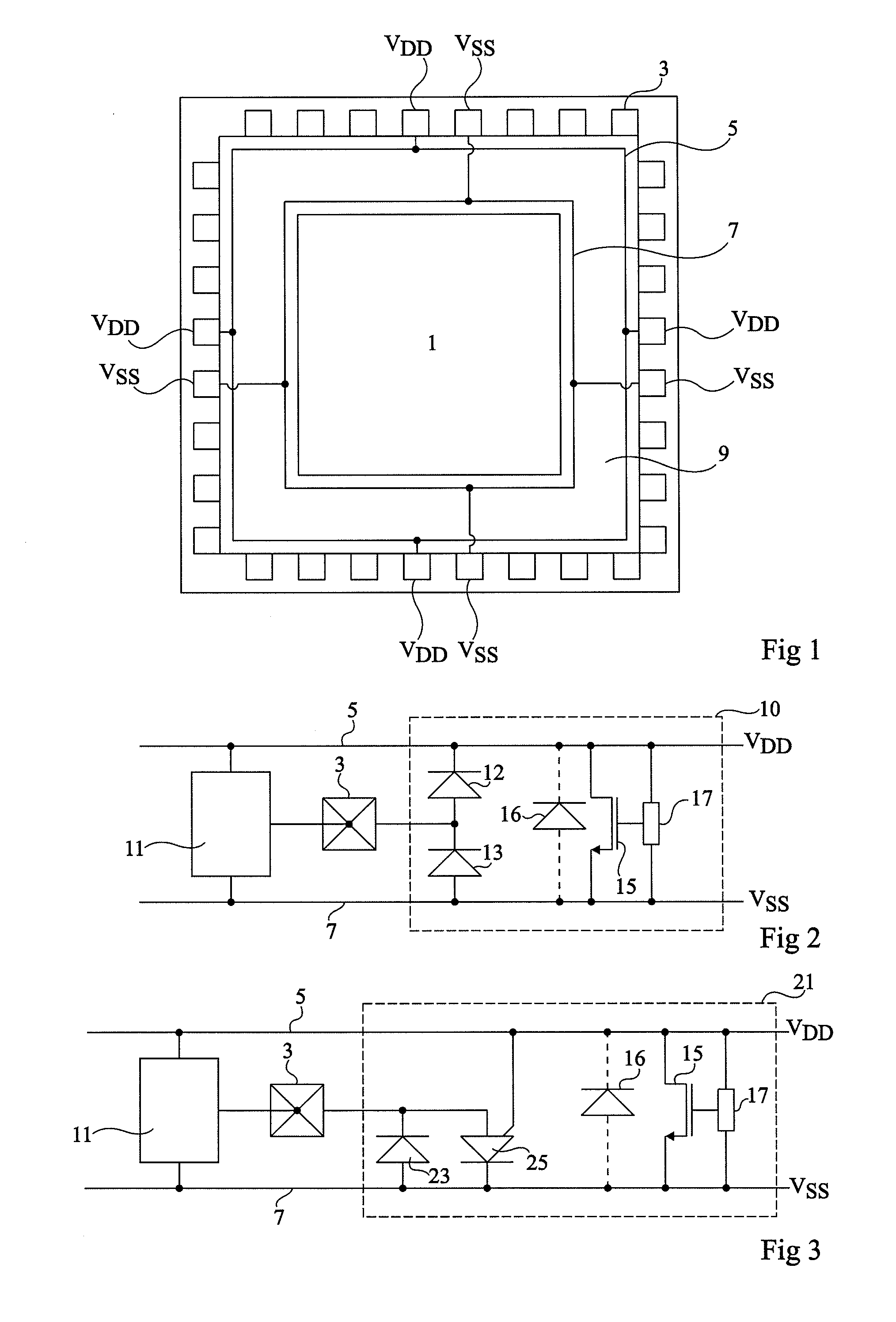
[0046]FIG. 3 shows the electric diagram of an example of a structure of protection against overvoltages 21, associated with an input / output pad 3 of an integrated circuit. A block 11 connected to pad 3 and to positive and negative power supply rails 5 and 7, symbolizes circuit elements protected by structure 21 against possible electrostatic discharges.

[0047]Like protection structure 10 described in relation with FIG. 2, structure 21 comprises a MOS transistor 15, used as a switch, connected between rails 5 and 7. An overvoltage detection circuit 17, connected in parallel with MOS transistor 15, provides a trigger signal to this transistor. MOS transistor 15 especially comprises a parasitic diode 16 forward-connected between rail 7 and rail 5.

[0048]A diode 23 is ...


PUM


Abstract

A structure for protecting an integrated circuit against electrostatic discharges, including a device for removing overvoltages between first and second power supply rails; and a protection cell connected to a pad of the circuit including a diode having an electrode, connected to a region of a first conductivity type, connected to the second power supply rail and having an electrode, connected to a region of a second conductivity type, connected to the pad and, in parallel with the diode, a thyristor having an electrode, connected to a region of the first conductivity type, connected to the pad and having a gate, connected to a region of the second conductivity type, connected to the first rail, the first and second conductivity types being such that, in normal operation, when the circuit is powered, the diode is non-conductive.

Description

CROSS REFERENCE TO RELATED APPLICATIONS [0001]This application claims the priority benefit of French patent application number 09 / 55757, filed on Aug. 24, 2009, entitled “STRUCTURE FOR PROTECTING AN INTEGRATED CIRCUIT AGAINST ELECTROSTATIC DISCHARGES” which is hereby incorporated by reference to the maximum extent allowable by law.BACKGROUND OF THE INVENTION [0002]1. Field of the Invention[0003]The present invention relates to structures for protecting integrated circuits against electrostatic discharges.[0004]2. Discussion of the Related Art[0005]FIG. 1 is a simplified top view of an integrated circuit chip. The integrated circuit comprises a central portion 1 connected to an assembly of metal pads 3 arranged at the chip periphery and intended to provide connections to the outside. Central portion 1 comprises all the components enabling the integrated circuit to perform desired functions. Some of pads 3 are intended to receive positive (VDD) and negative (VSS) supply voltages. Posi...

Claims


Application Information

Patent Timeline
Patent Type & Authority Applications(United States)
IPC IPC(8): H01L29/78
CPCH01L27/0262H01L29/0649H01L29/0692H01L29/8611H01L29/7436
Inventor GALY, PHILIPPEENTRINGER, CHRISTOPHEJIMENEZ, JEAN
Owner STMICROELECTRONICS SRL
Why Eureka
Try Eureka