Thin film deposition apparatus and method of manufacturing organic light-emitting display device by using the same

a technology of thin film deposition and manufacturing method, which is applied in mechanical equipment, sleeve/socket joints, transportation and packaging, etc., can solve the problems of fmms having disadvantages with respect to the current trend of high pitch patterning, pattern distortion, and disadvantages of fmms

Active Publication Date: 2011-02-24
SAMSUNG DISPLAY CO LTD
View PDF42 Cites 51 Cited by
  • Summary
  • Abstract
  • Description
  • Claims
  • Application Information

AI Technical Summary

Benefits of technology

[0009]Aspects of the present invention provide a thin film deposition apparatus that may be simply applied to manufacture large display devices on a mass scale and whi

Problems solved by technology

However, it is disadvantageous to use an FMM when manufacturing organic light-emitting display devices on a large scale using a large sized mother-glass.
When a large mask, such as an FMM, is used for deposition onto a large sized mother-glass, the mask is likely to bend due to the weight thereof, thereby causing a pattern to be distort

Method used


Image

  • Thin film deposition apparatus and method of manufacturing organic light-emitting display device by using the same
  • Thin film deposition apparatus and method of manufacturing organic light-emitting display device by using the same
  • Thin film deposition apparatus and method of manufacturing organic light-emitting display device by using the same

Examples


Embodiment Construction

[0053]Reference will now be made in detail to the present embodiments of the present invention, examples of which are illustrated in the accompanying drawings, wherein like reference numerals refer to the like elements throughout. The embodiments are described below in order to explain the present invention by referring to the figures.

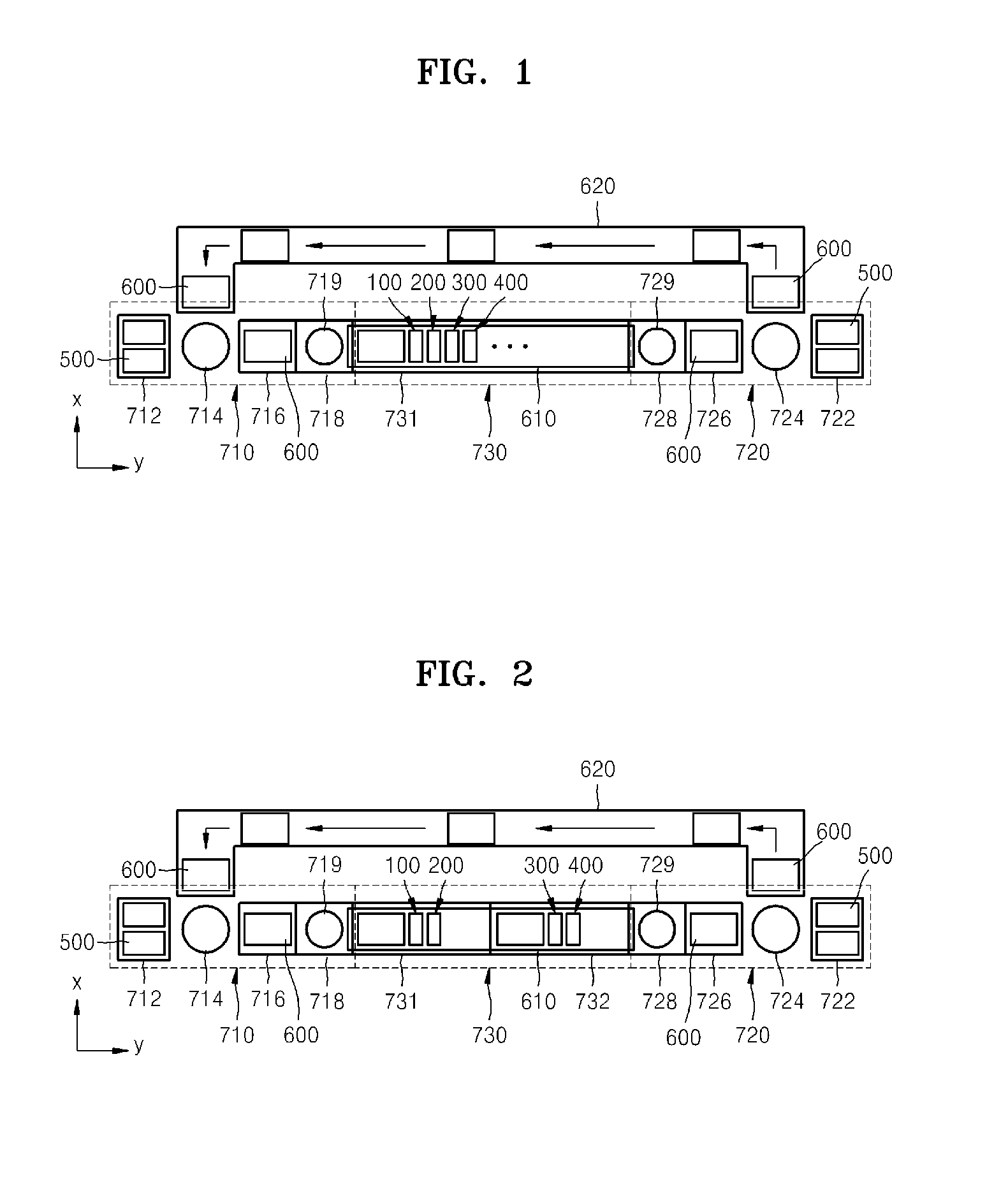
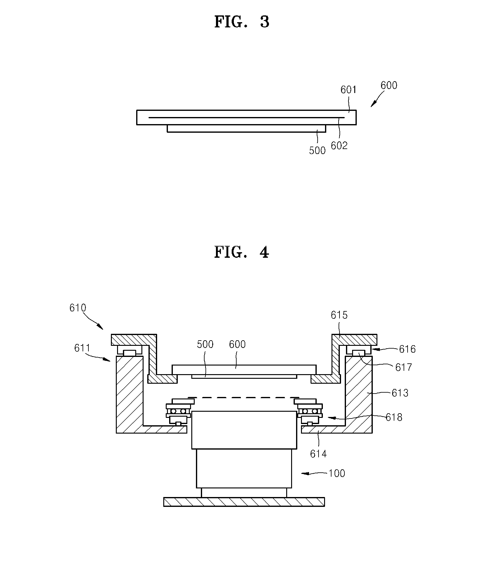
[0054]FIG. 1 is a schematic view of a thin film deposition apparatus according to another embodiment of the present invention. FIG. 2 is a schematic view of a thin film deposition apparatus 1 according to another embodiment of the present invention. FIG. 3 is a schematic view of an electrostatic chuck 600 included in the thin film deposition apparatus of FIG. 1 or 2, according to an embodiment of the present invention.

[0055]In particular and referring to FIG. 1, the thin film deposition apparatus according to the current embodiment includes a loading unit 710, an unloading unit 720, a deposition unit 730, a first circulating unit 610, and a second circ...


PUM

PropertyMeasurementUnit
Angleaaaaaaaaaa
Poweraaaaaaaaaa
Timeaaaaaaaaaa

Abstract

A thin film deposition apparatus and an organic light-emitting display device by using the same. The thin film deposition apparatus includes an electrostatic chuck, an a plurality of chambers; at least one thin film deposition assembly; a carrier; a first power source plug; and a second power source plug. The electrostatic chuck includes a body having a supporting surface that contacts a substrate to support the substrate, wherein the substrate is a deposition target; an electrode embedded into the body and applying an electrostatic force to the supporting surface; and a plurality of power source holes formed to expose the electrode and formed at different locations on the body. The plurality of chambers are maintained in a vacuum state. The at least one thin film deposition assembly is located in at least one of the plurality of chambers, is separated from the substrate by a predetermined distance, and is used to form a thin film on the substrate supported by the electrostatic chuck. The carrier is used to move the electrostatic chuck to pass through the plurality of chambers. The first power source plug is installed to be attachable to and detachable from one of the power source holes in order to supply power to the electrode. The first power source plug is installed at an upstream of a path in which the electrostatic chuck is moved by the carrier. The second power source plug is installed to be attachable to and detachable from another of the power source holes in order to supply power to the electrode. The second power source plug is installed in the path to be downstream to the first power source plug with respect to the path.

Description

CROSS-REFERENCE TO RELATED APPLICATIONS[0001]This application claims the benefit of Korean Application No(s). 10-2009-0078175, filed Aug. 24, 2009 and 10-2010-0011479 filed Feb. 8, 2010, in the Korean Intellectual Property Office, the disclosures of which are incorporated herein by reference.BACKGROUND OF THE INVENTION[0002]1. Field of the Invention[0003]Aspects of the present invention relate to a thin film deposition apparatus and a method of manufacturing an organic light-emitting display device by using the same, and more particularly, to a thin film deposition apparatus that can be simply applied to manufacture large display devices on a mass scale, and a method of manufacturing an organic light-emitting display device by using the thin film deposition apparatus.[0004]2. Description of the Related Art[0005]Organic light-emitting display devices have a larger viewing angle, better contrast characteristics, and a faster response rate than other display devices, and thus have draw...

Claims


Application Information

Patent Timeline
IPC IPC(8): H01L33/26C23C16/44
CPCC23C14/044C23C14/12C23C14/243C23C14/568Y10T279/23H01L51/0081H01L51/56Y10S414/135H01L51/001H10K71/164H10K85/324H10K71/00
Inventor KANG, HEE-CHEOLPARK, HYUN-SOOKRYU, JAE-KWANGCHOL, YONG-SUPLEE, YUN-MLKIM, SANG-SOO
Owner SAMSUNG DISPLAY CO LTD
Why Eureka
Try Eureka