Multi-film stack etching with polymer passivation of an overlying etched layer

a polymer passivation and etching technology, applied in the field of thin film plasma etching, can solve the problems of increasing the complexity of the etching process used to pattern such stacks, and the generality of multi-film stacks, and achieve the effect of reducing erosion

Inactive Publication Date: 2011-02-24
APPLIED MATERIALS INC
View PDF10 Cites 22 Cited by
  • Summary
  • Abstract
  • Description
  • Claims
  • Application Information

AI Technical Summary

Benefits of technology

[0013]Plasma etching of a multi-film stack with passivation is described. A method and apparatus for plasma etching a workpiece, such as a semiconductor wafer, including a thin film stack having a top (first) film disposed over a bottom (third) film with an intervening middle (second) film there between is described for particular embodiments of the present invention. A first carbon-lean gas chemistry is used to etch through the top film, a second carbon-lean gas chemistry is used to etch through the middle film, and the bottom film is etched through by alternating between depositing a polymer passivation on the top film using a carbon-rich gas chemistry and an etching of the bottom film with a third carbon-lean gas chemistry, which may be the same as the first carbon-lean gas chemistry. Where etch selectivity between the top and bottom films may be as low as between 1:1 and 2:1, the iterative deposition and etching is clears the bottom film with reduced erosion of the top and / or middle films.

Problems solved by technology

While such vertically integrated multi-film stacks may be advantageous for a number of reasons, such multi-film stacks generally can increase the complexity of etch processes used to pattern such stacks with a particular masking pattern.

Method used


Image

  • Multi-film stack etching with polymer passivation of an overlying etched layer
  • Multi-film stack etching with polymer passivation of an overlying etched layer
  • Multi-film stack etching with polymer passivation of an overlying etched layer

Examples


Embodiment Construction

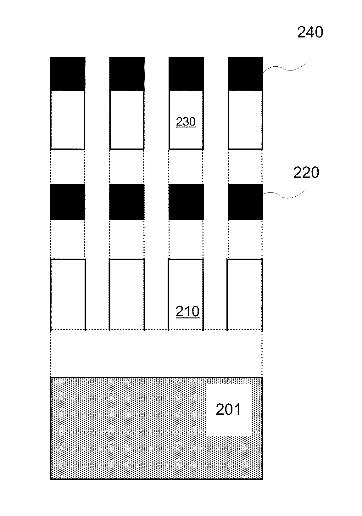
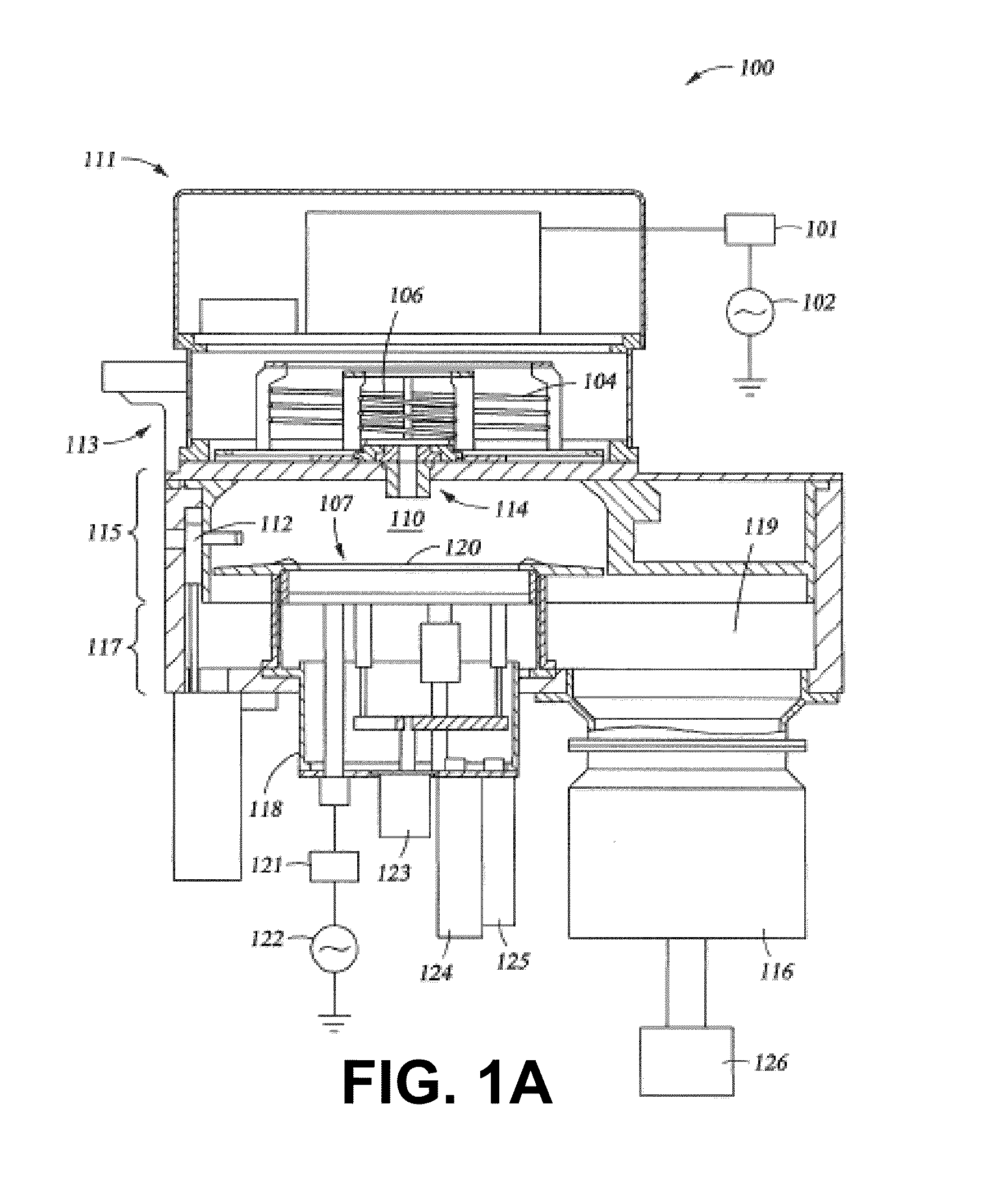
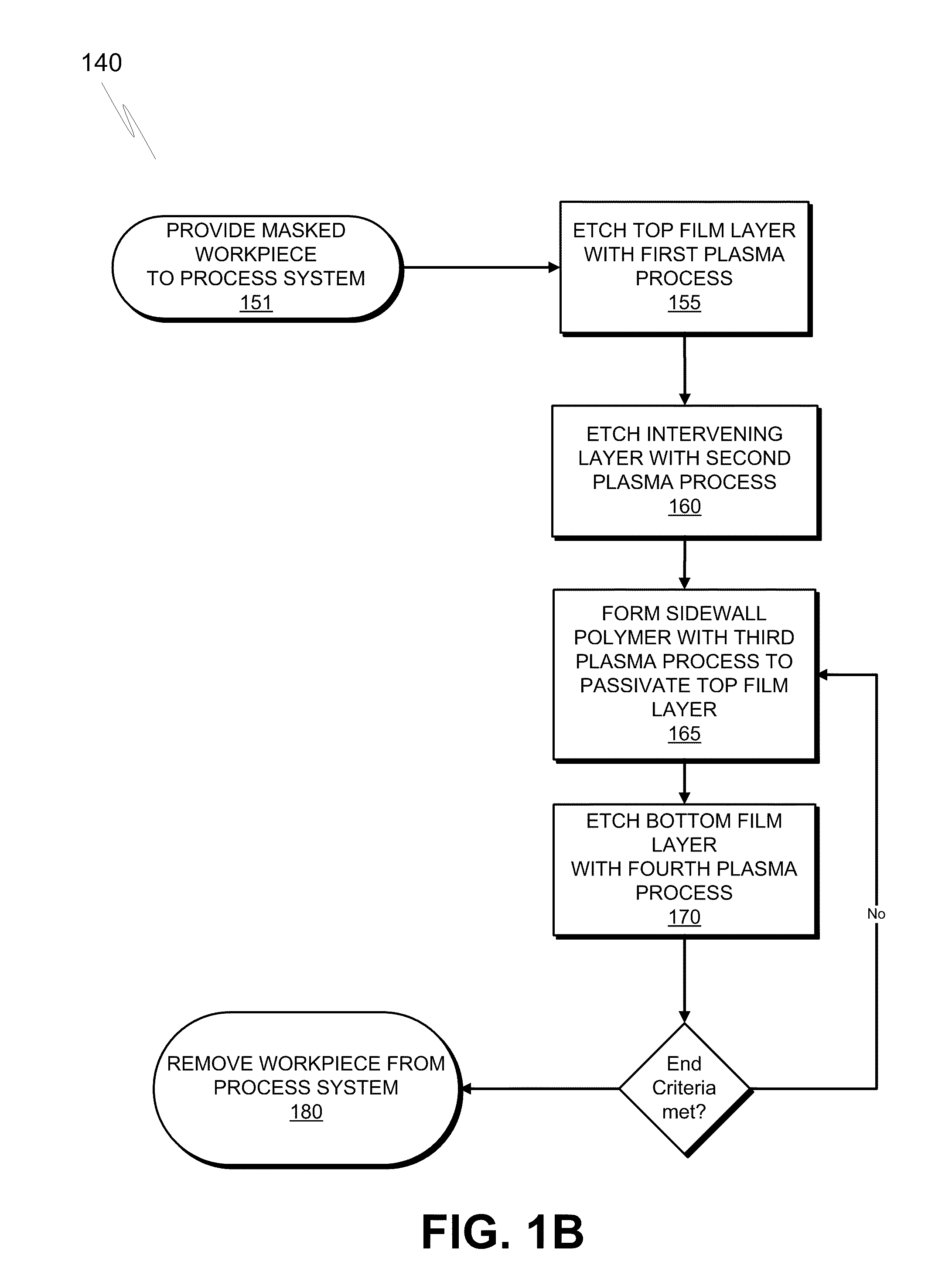
[0015]Plasma etching of a multi-film stack with passivation is described. In the following description, numerous specific details are set forth, such as fabrication conditions and materials, in order to provide a thorough understanding of the present invention. It will be apparent to one skilled in the art that the present invention may be practiced without these specific details. In other instances, well-known features, such as lithographic mask patterning and thin film deposition, are not described in detail in order to not unnecessarily obscure the present invention. Furthermore, it is to be understood that the various embodiments shown in the Figures are merely illustrative representations.

[0016]The terms “over,”“under,”“between,” and “on” as used herein refer to a relative position of one member with respect to other members. As such, for example, one member disposed over or under another member may be directly in contact with the other member or may have one or more intervenin...


PUM

PropertyMeasurementUnit
RF bias poweraaaaaaaaaa
diameter sizeaaaaaaaaaa
frequenciesaaaaaaaaaa

Abstract

A method and apparatus for plasma etching a workpiece, such as a semiconductor wafer, including a thin film stack having a top film disposed over a bottom film with an intervening middle film there between. Etch selectivity between the top and bottom films may be as low as between 1:1 and 2:1 and a first carbon-lean gas chemistry is used to etch through the top film, a second carbon-lean gas chemistry is used to etch through the middle film, and the bottom film is etched through by alternating between depositing a polymer passivation on the top film using a carbon-rich gas chemistry and an etching of the bottom film with a third carbon-lean gas chemistry, which may be the same as the first carbon-lean gas chemistry.

Description

CROSS REFERENCE TO RELATED APPLICATIONS[0001]This application is related to, and claims priority to, the provisional utility application entitled “MULTI-FILM STACK ETCHING WITH POLYMER PASSIVATION OF AN OVERLYING ETCHED LAYER,” filed on Aug. 20, 2009, having an application number of 61 / 235,651 and herein incorporated by reference in its entirety for all purposes.BACKGROUND[0002]1) Field[0003]Embodiments of the present invention pertain to the field of thin-film plasma etching and, in particular, to multi-film stack plasma etching with polymer passivation.[0004]2) Description of Related Art[0005]Recent efforts towards scaling the dimensions of semiconductor devices have include highly integrated film stack having a multiplicity of thin film layers. Such multi-film stacks find wide utility in wide array of microelectronic devices, such microprocessors, volatile and non-volatile memories, MEMS, and three-dimensionally integrated active device structures in which the vertical dimension ...

Claims


Application Information

Patent Timeline
Patent Type & Authority Applications(United States)
IPC IPC(8): H01L21/3065C23F1/08
CPCC23F4/00H01J37/32449H01L21/32136H01L27/0688H01L21/32139H01L21/67069H01L21/32137
Inventor SRINIVASAN, SUNILCHOI, JINHANKHAN, ANISUL H.
Owner APPLIED MATERIALS INC
Why Eureka
Try Eureka