

Epitaxial substrate for semiconductor device, semiconductor device, and method of manufacturing epitaxial substrate for semiconductor device
- Summary
- Abstract
- Description
- Claims
- Application Information
AI Technical Summary
Benefits of technology
Problems solved by technology
Method used
Image

Examples
first preferred embodiment
[0026]Configuration of HEMT Device
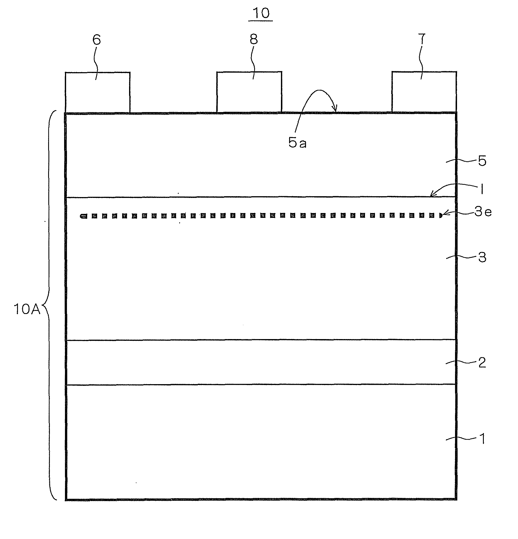
[0027]FIG. 1 is a schematic cross-sectional view schematically showing the configuration of a HEMT device 10 according to a first preferred embodiment of the present invention. The HEMT device 10 has the configuration in which a substrate 1, a buffer layer 2, a channel layer 3 and a barrier layer 5 are formed by lamination. The buffer layer 2, the channel layer 3 and the barrier layer 5 are preferred examples of layers that are epitaxially formed (details thereof are described below) using the metal organic chemical vapor deposition method (MOCVD method). Hereinbelow, the laminated structure formed by laminating the substrate 1, the buffer layer 2, the channel layer 3 and the barrier layer 5 is also referred to as an epitaxial substrate 10A. Note that ratios of respective layers in FIG. 1 do not reflect actual ones.
[0028]Hereinbelow, while description is given of a case where the MOCVD method is used for the formation of each layer, other epitaxial ...
second preferred embodiment
[0083]HEMT Device Including Spacer Layer
[0084]FIG. 7 is a schematic cross-sectional diagram schematically showing the configuration of a HEMT device 20 according to a second preferred embodiment of the present invention. The HEMT device 20 has the configuration in which a spacer layer 4 is interposed between the channel layer 3 and the barrier layer 5 of the HEMT device 10 according to the first preferred embodiment. Constituent elements other than the spacer layer 4 are the same as those of the HEMT device 10 according to the first preferred embodiment, and thus detailed description thereof is omitted. Note that the laminated structure in which the substrate 1, the buffer layer 2, the channel layer 3, the spacer layer 4 and the barrier layer 5 are formed by lamination is also referred to as an epitaxial substrate 20A.
[0085]The spacer layer 4 is formed of a group III nitride that has a composition of Inx3Aly3Gaz3N (x3+y3+z3=1), contains at least Al, and has a bandgap equal to or lar...
##ventive example 1
Inventive Example 1
[0098]In this inventive example, six types (samples No. 1 to No. 6) of epitaxial substrates that have different In composition distribution in the near-surface portion of the barrier layer were manufactured, and ohmic contact characteristics thereof were evaluated.
[0099]In manufacturing an epitaxial substrate, first, a plurality of 6H—SiC substrates that have (0001) plane orientation and a diameter of three inches were prepared as the substrate. Each of the substrates was placed in a reactor of an MOCVD reactor, and an inside of the reactor was replaced with vacuum gas. After that, a pressure inside the reactor was set to 30 kPa, thereby forming the atmosphere in hydrogen / nitrogen mixed flow state. Then, a temperature of the substrate was raised through susceptor heating.
[0100]When a susceptor temperature reached 1,050° C., Al source gas and ammonia gas were introduced into the reactor, to thereby form an AlN layer that serves as the buffer layer and has a thickne...
PUM
 Abstract
Description
Claims
Application Information