Epitaxial substrate for semiconductor device, semiconductor device, and method of manufacturing epitaxial substrate for semiconductor device

a semiconductor device and epitaxial substrate technology, applied in the direction of semiconductor devices, basic electric elements, electrical apparatus, etc., to achieve the effect of satisfactory device characteristics and excellent schottky contact characteristics

Active Publication Date: 2013-04-02
NGK INSULATORS LTD
View PDF4 Cites 5 Cited by
  • Summary
  • Abstract
  • Description
  • Claims
  • Application Information

AI Technical Summary

Benefits of technology

[0011]According to the present invention, there is achieved a semiconductor device having schottky contact characteristics between a barrier layer and an electrode being in schottky contact therewith, which are more improved compared with a conventional case.
[0012]Therefore, an object of the present invention is to provide an epitaxial substrate for semiconductor device that is capable of achieving a semiconductor device having excellent schottky contact characteristics and satisfactory device characteristics.

Problems solved by technology

In order to put the above-mentioned HEMT device or a substrate for HEMT device that is a multi-layer structure used in manufacturing the same to practical use, various problems need to be solved; problems related to performance improvement such as increase of power density and efficiency, problems related to functional improvement such as achieving normally-off operation, and fundamental problems such as enhancing reliability and reducing cost.
One of the above-mentioned problems is to improve schottky contact characteristics between a gate electrode and a barrier layer.

Method used


Image

  • Epitaxial substrate for semiconductor device, semiconductor device, and method of manufacturing epitaxial substrate for semiconductor device
  • Epitaxial substrate for semiconductor device, semiconductor device, and method of manufacturing epitaxial substrate for semiconductor device
  • Epitaxial substrate for semiconductor device, semiconductor device, and method of manufacturing epitaxial substrate for semiconductor device

Examples


##ventive example 1

Inventive Example 1

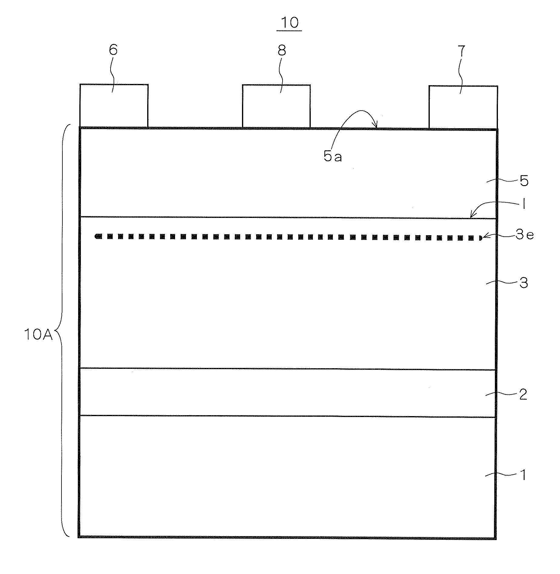
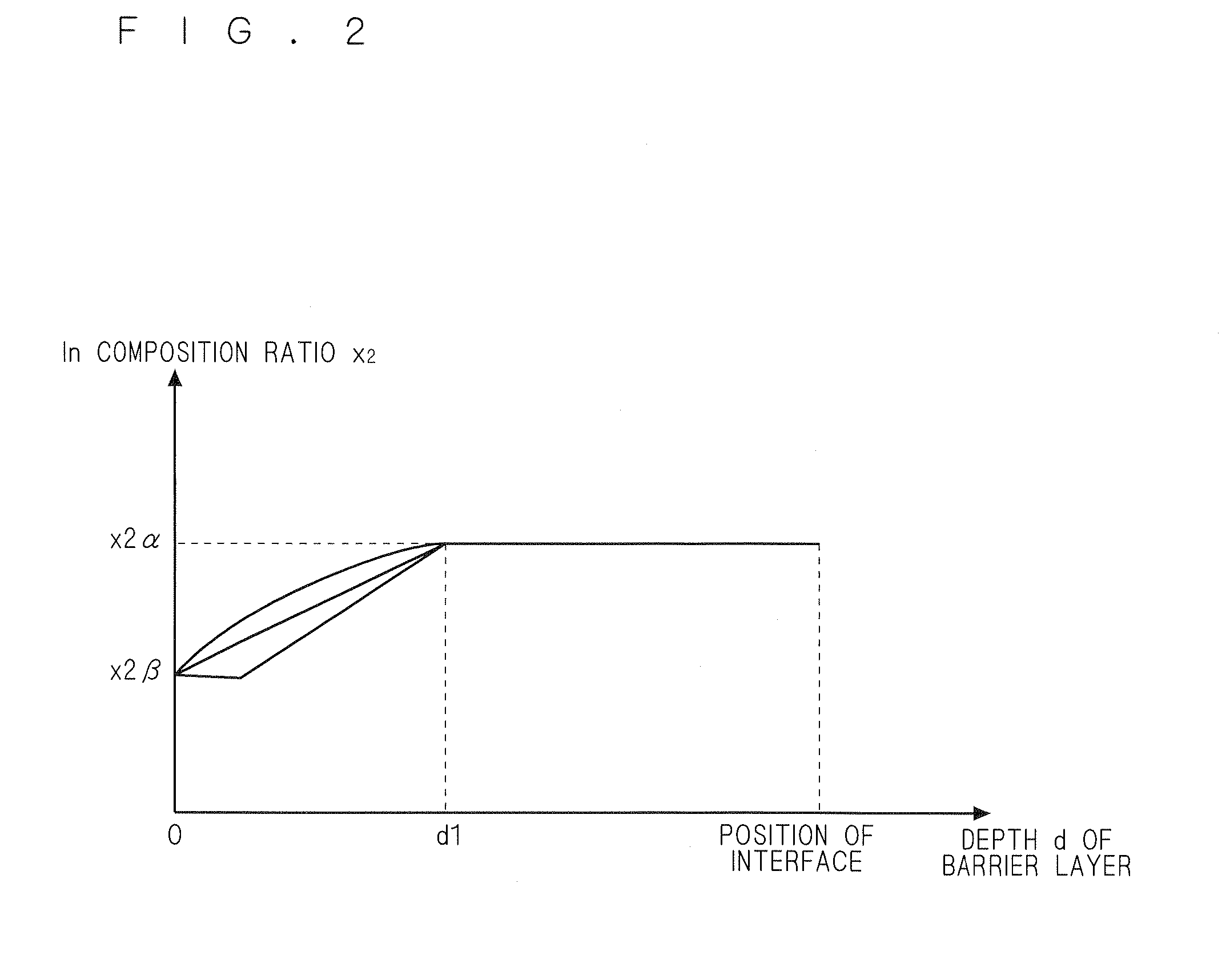
[0099]In this inventive example, six types (samples No. 1 to No. 6) of epitaxial substrates that have different In composition distribution in the near-surface portion of the barrier layer were manufactured, and schottky contact characteristics thereof were evaluated.

[0100]In manufacturing an epitaxial substrate, first, a plurality of 6H—SiC substrates that have (0001) plane orientation and a diameter of three inches were prepared as the substrate. Each of the substrates was placed in a reactor of an MOCVD reactor, and an inside of the reactor was replaced with vacuum gas. After that, a pressure inside the reactor was set to 30 kPa, thereby forming the atmosphere in hydrogen / nitrogen mixed flow state. Then, a temperature of the substrate was raised through susceptor heating.

[0101]When a susceptor temperature reached 1,050° C., Al source gas and ammonia gas were introduced into the reactor, to thereby form an AlN layer that serves as the buffer layer and has a thic...


PUM

PropertyMeasurementUnit
depthaaaaaaaaaa
thicknessaaaaaaaaaa
thicknessaaaaaaaaaa

Abstract

Provided is an epitaxial substrate capable of achieving a semiconductor device that has excellent schottky contact characteristics as well as satisfactory device characteristics. On a base substrate, a channel layer formed of a first group III nitride that contains at least Al and Ga and has a composition of Inx1Aly1Gaz1N (x1+y1+z1=1) is formed. On the channel layer, a barrier layer formed of a second group III nitride that contains at least In and Al and has a composition of Inx2Aly2Gaz2N (x2+y2+z2=1) is formed such that an In composition ratio of a near-surface portion is smaller than an In composition ratio of a portion other than the near-surface portion.

Description

FIELD OF THE INVENTION[0001]The present invention relates to an epitaxial substrate that has a multi-layer structure composed of a group III nitride semiconductor, and more particularly, to a multi-layer structured epitaxial substrate for electronic devices and a method of manufacturing the same.BACKGROUND OF THE INVENTION[0002]Nitride semiconductors having high breakdown electric field and high saturation electron velocity have been attracting attention as the next generation of semiconductor materials for high-frequency / high-power devices. For example, a high electron mobility transistor (HEMT) device formed by laminating a barrier layer composed of AlGaN and a channel layer composed of GaN takes advantage of the feature that high-concentration two-dimensional electron gas (2DEG) is generated at a lamination interface (hetero interface) owing to a polarization effect (spontaneous polarization effect and piezo polarization effect) inherent in a nitride material (for example, see “H...

Claims


Application Information

Patent Timeline
Patent Type & Authority Patents(United States)
IPC IPC(8): H01L29/66
CPCH01L29/2003H01L29/7787H01L29/66462H01L29/201
Inventor MIYOSHI, MAKOTOKURAOKA, YOSHITAKASUMIYA, SHIGEAKIICHIMURA, MIKIYASUGIYAMA, TOMOHIKOTANAKA, MITSUHIRO
Owner NGK INSULATORS LTD
Why Eureka
Try Eureka