Method of manufacturing semiconductor element

a manufacturing method and semiconductor technology, applied in the direction of semiconductor devices, electrical devices, transistors, etc., can solve the problems of inability to use the sheet, the p-layer cannot be highly activated, and the traces of work damage caused by laser irradiation can be found on the surface of the wafer, so as to suppress the increase in the temperature of the substrate, prevent the occurrence of device failure, and reduce the cooling effect by heat conduction to the stage

Active Publication Date: 2008-09-18
FUJI ELECTRIC CO LTD
View PDF11 Cites 17 Cited by
  • Summary
  • Abstract
  • Description
  • Claims
  • Application Information

AI Technical Summary

Benefits of technology

[0035]When the substrate is afloat from the stage during laser irradiation, the cooling effect by heat conduction to the stage is decreased, which causes the temperature of the substrate to rise. However, by irradiating a laser beam while the wafer is fixed to an electrostatic chuck stage, it is possible to suppress the increase in temperature of the substrate during laser irradiation. This effect is noticeable with a thin wafer having a thickness on the order of 70 μm. In particular, when lithium is used as a dopant, this configuration is preferable because diffusion of lithium can be controlled by keeping the temperature of the substrate during laser irradiation below 100° C.
[0036]According to the method of manufacturing a semiconductor element of the invention, it is possible to achieve the advantage that the occurrence of device failure can be prevented. Also, it is possible to achieve another advantage in that a semiconductor element having satisfactory device characteristics can be manufactured. Further, it is possible to achieve still another advantage in that breakage of the device by heat induced during laser irradiation can be prevented.

Problems solved by technology

However, an alternating current input requires a semiconductor switch to have a high reverse breakdown voltage.
In activating the p-layer and the n-layer in the case of previous electric furnace annealing, however, the p-layer cannot be made highly activated.
Furthermore, in the method of using an adhesive sheet for preventing cracking of the wafer, the permissible temperature of the adhesive sheet is usually 200° C. or less which makes the use of the sheet impossible when the electric furnace annealing needs to be carried out at 300° C. or more.
Moreover, when one irradiation area is irradiated with a laser beam in which irradiation energy density has been increased, traces of work damage by the laser irradiation sometime remain on the surface of the wafer.
In the case where these layers are formed shallow, flaws or adhesion of dirt frequently occurs on the bottom surface of the substrate during the process steps.
Leakage current increases when the n-buffer layer is not formed properly in part because of such flaws or dirt.
This raises the problem that device failure readily occurs.
In addition, in the case where a dopant having a large diffusion coefficient is used, the dopant penetrates through the substrate and comes off of the substrate when heat treatment for diffusion and activation is carried out for a long time.
This raises another problem in that a desired characteristic cannot be achieved in a stable manner.
This raises still another problem of a broken device.

Method used


Image

  • Method of manufacturing semiconductor element
  • Method of manufacturing semiconductor element
  • Method of manufacturing semiconductor element

Examples


first embodiment

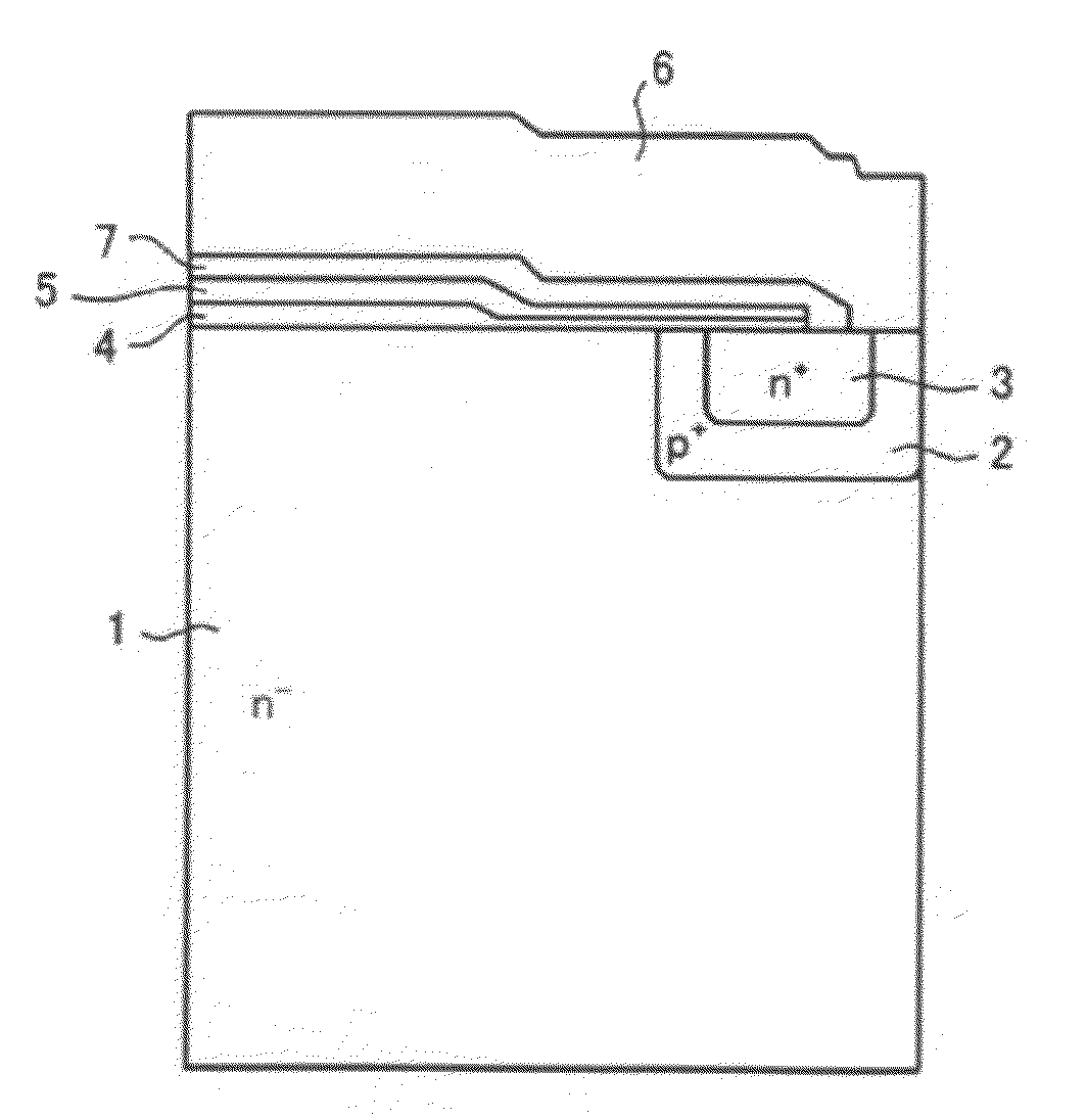
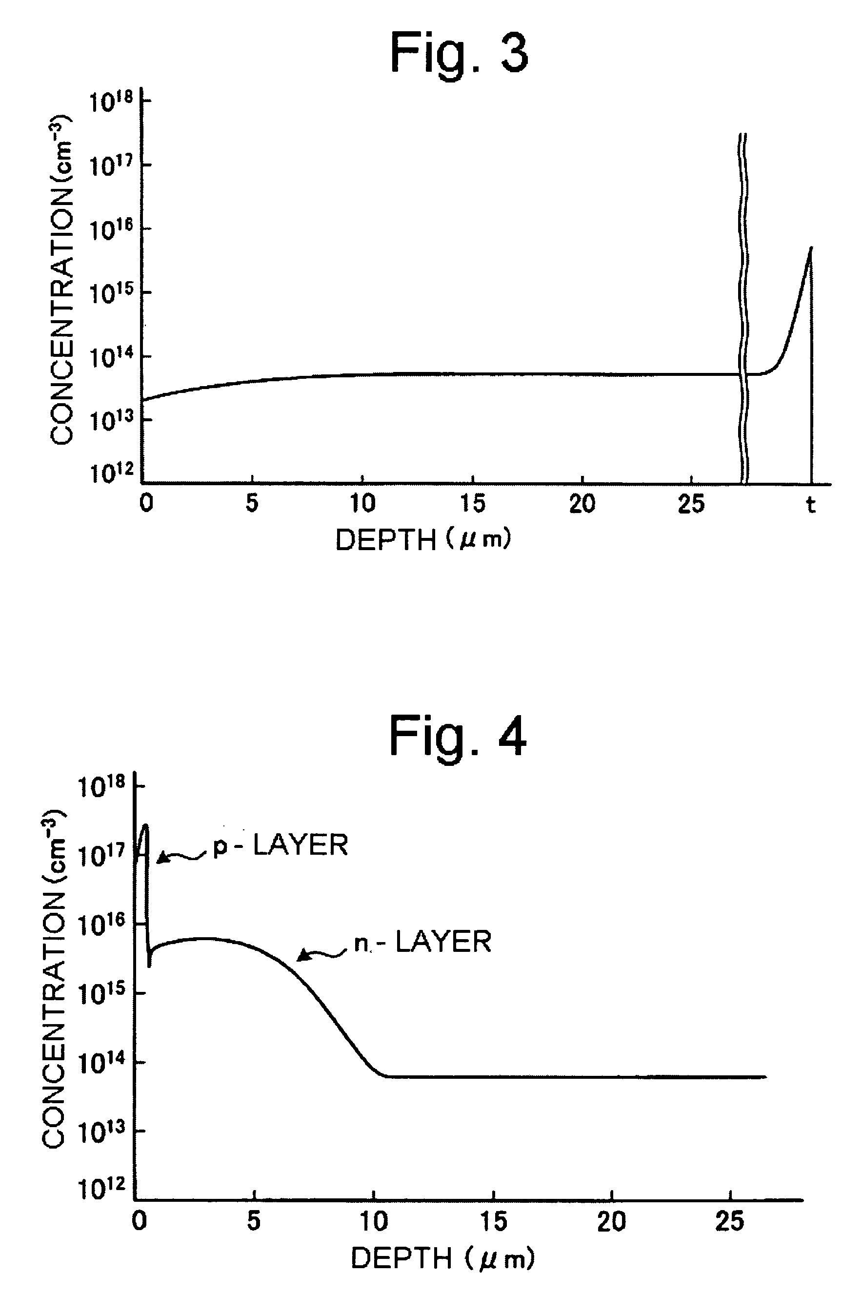
[0057]A first embodiment uses lithium as a dopant to form n+-layer 10a in the ion-implantation step to form an n-buffer layer and a p+-collector layer as shown in FIG. 16. In the case where the n+-layer 10a and the p+-layer 8a are activated and a top surface contact layer coming into contact with the bottom surface electrode is provided following this ion-implantation step, two all-solid-state YAG2ω lasers (wavelength: 532 nm) are used to carry out laser annealing in the step of activating the top surface contact layer.

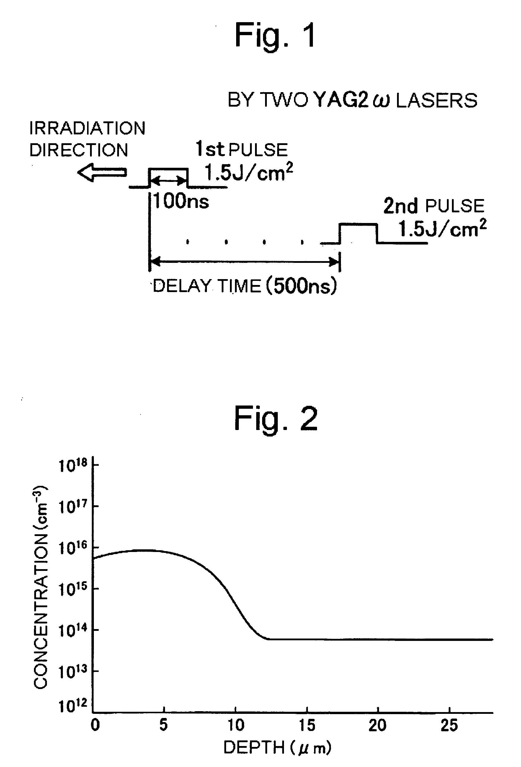
[0058]FIG. 1 is a view showing a pulse shape of a pulsed laser beam irradiated from each of the two laser irradiation devices. As is shown in FIG. 1, when laser beams are irradiated, the full-width at half maximum (corresponding to pulse width) of the both two lasers is, for example, 100 ns. Also, the irradiation energy density of each of the first laser (first pulse) and the second laser (second pulse) is, for example, 1.5 J / cm2, so that the laser irradiation energy ...

second embodiment

[0064]In a second embodiment, a semiconductor laser (wavelength: 800 nm) is used instead of one of the two all-solid-state YAG2ω lasers (wavelength: 532 nm) used in the first embodiment. Lithium is used as a dopant to form the n+-layer 10a.

[0065]FIG. 5 is a view showing the pulse shape of a pulsed laser beam irradiated from the all-solid-state YAG2ω laser and the continuous oscillation of the semiconductor laser. As shown in FIG. 5, when laser beams are irradiated, the full-width at half maximum (corresponding to the pulse width) of the all-solid-state YAG2ω laser is, for example, 100 ns. Also, the irradiation energy density of the all-solid-state YAG2ω laser is, for example, 1.5 J / cm2. During wafer processing, a laser beam is irradiated to the entire wafer surface from the semiconductor laser at an irradiation energy density of, for example, 5 J / cm2. Also, the overlapping ratio of the pulses of the all-solid-state YAG2ω laser is, for example, 90%,

[0066]These laser irradiation cond...


PUM


Abstract

A method of manufacturing a semiconductor element includes implanting ions of a dopant having a large diffusion coefficient into a semiconductor to provide a doped layer; and irradiating the doped layer with a plurality of pulsed laser beams supplied by a plurality of laser irradiation devices to activate the doped layer and provide an activated doped layer. The activated doped layer may be one of a single doped layer or a plurality of successive doped layers which each have respective conduction types that are one of identical or different. Device breakage and failure of the manufactured semiconductor element due to heat induced during laser irradiation are substantially prevented by this method.

Description

CROSS-REFERENCE TO RELATED APPLICATION[0001]This Application claims the benefit of priority from Japanese Published Application No. 2007-049087 filed Feb. 28, 2007, the contents of which are incorporated herein by reference.BACKGROUND OF THE INVENTION[0002]1. Field of the Invention[0003]The present invention relates to a method of manufacturing a semiconductor element, and more particularly, to a method of manufacturing a semiconductor element, such as an IC (Integrated Circuit), a MOS (Metal Oxide Semiconductor), and an insulated gate bipolar transistor (hereinafter, abbreviated to IGBT).[0004]2. Description of the Related Art[0005]In recent years, integrated circuits (ICs) have been most commonly used in important sections in a computer or a communication device. In such ICs, a number of transistors and resistors are connected so as to form electric circuits that are integrated onto one chip. Of these ICs, those including power semiconductor elements are referred to as power ICs.[...

Claims


Application Information

Patent Timeline
Patent Type & Authority Applications(United States)
IPC IPC(8): H01L21/225
CPCH01L21/26513H01L21/268H01L29/7395H01L29/66333H01L29/167H01L21/2658
Inventor NAKAZAWA, HARUO
Owner FUJI ELECTRIC CO LTD
Why Eureka
Try Eureka