Thin-film transistor based piezoelectric strain sensor and method

a piezoelectric strain sensor and thin film transistor technology, applied in the field of sensors and components, can solve the problems of large power consumption, low sensitivity large power consumption of traditional piezoresistive strain sensors, so as to improve sensitivity, reduce power consumption, and simplify electronics reading

Active Publication Date: 2011-03-03
HONEYWELL ROMANIA
View PDF13 Cites 52 Cited by
  • Summary
  • Abstract
  • Description
  • Claims
  • Application Information

AI Technical Summary

Benefits of technology

[0008]It is another aspect of the disclosed embodiments to provide for an improved field-effect piezoelectric strain sensor apparatus for detecting strain, vibration, force, and / or pressure.
[0009]It is a further aspect of the disclosed embodiments to provide for an improved method for fabricating a strain sensor apparatus on a flexible substrate utilizing a low cost fabrication technique.
[0011]The apparatus can be formed as a single gate field-effect piezoelectric sensor and / or a dual gate field-effect piezoelectric sensor. The semiconductor layer (e.g. Si, SnO2, In2O3, ZnO, InN, AlInN, etc.) can be formed from a nanowire array, resulting in a metal-piezoelectric-nanowire field-effect transistor. Such a single and dual gate field-effect piezoelectric sensor configurations offer increased sensitivity and device control (i.e., dual gate configuration) due to the presence of the piezoelectric layer in the transistor structure and a low cost manufacturability with respect to the large area flexible substrate.

Problems solved by technology

The majority of prior art strain sensors are not suitable for manufacturing on a flexible substrate.
Such strain sensors, if based on piezoelectric materials, also require complex electronics for collecting the sensor signal and operate with a low sensitivity.
Traditional piezoresistive strain sensors have either a very low sensitivity (e.g., metallic sensors) or large power consumption (e.g., semiconductor piezoresistive sensors).
Furthermore, the cost for manufacturing such sensors on a substrate increases the complexity of the resulting system and may result in a reduction in reliability.

Method used


Image

  • Thin-film transistor based piezoelectric strain sensor and method
  • Thin-film transistor based piezoelectric strain sensor and method
  • Thin-film transistor based piezoelectric strain sensor and method

Examples


Embodiment Construction

[0025]The particular values and configurations discussed in these non-limiting examples can be varied and are cited merely to illustrate at least one embodiment and are not intended to limit the scope thereof.

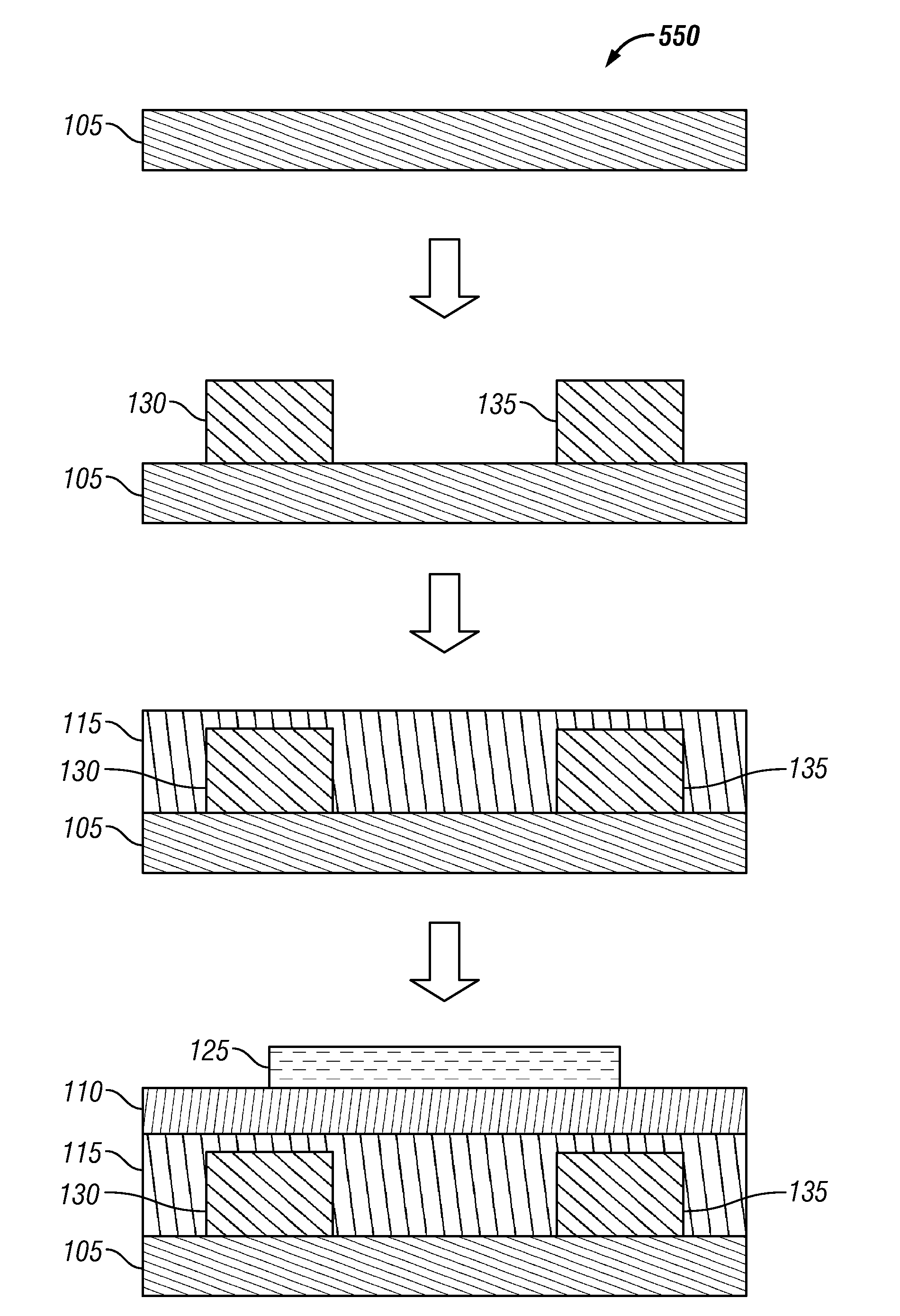
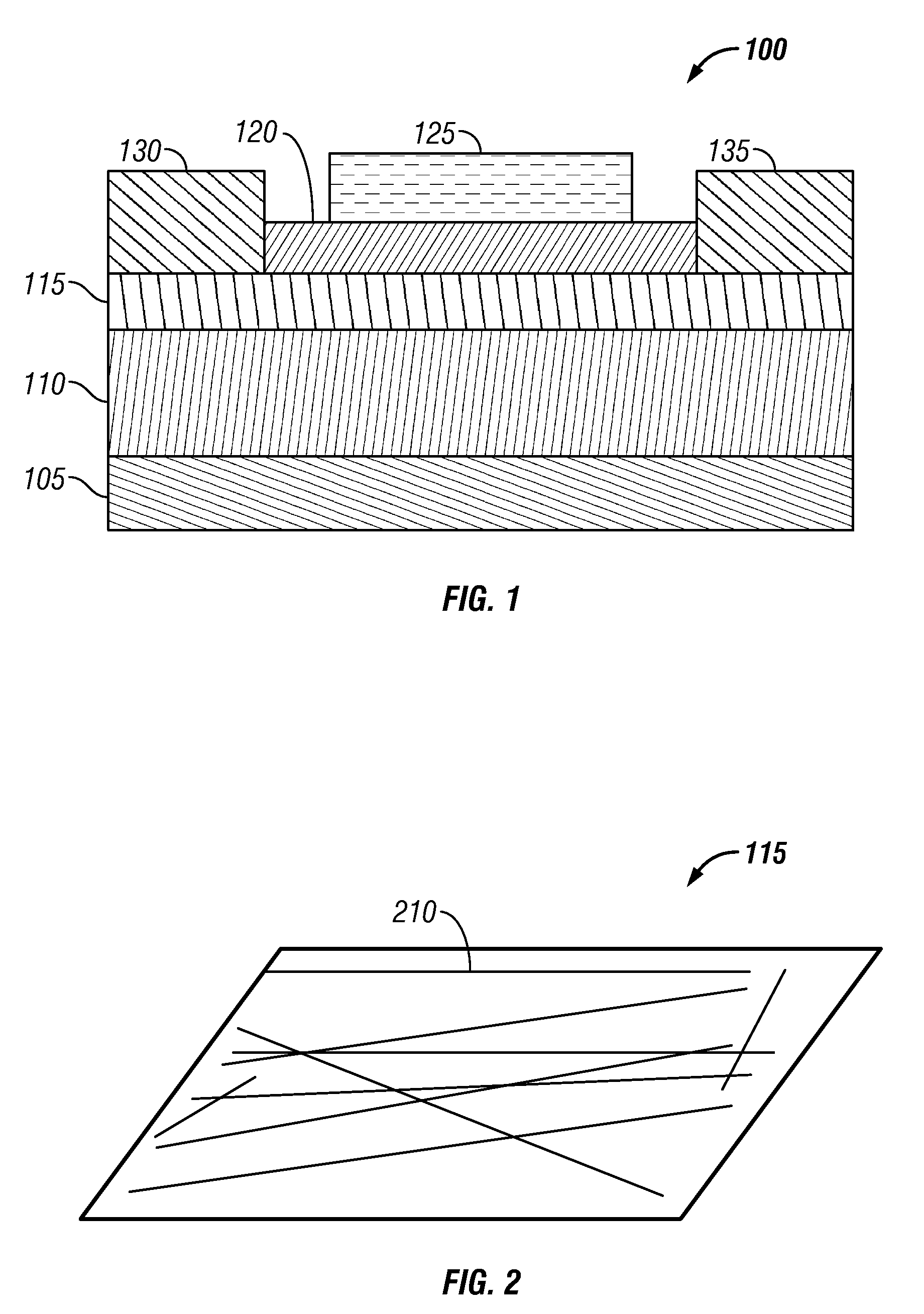
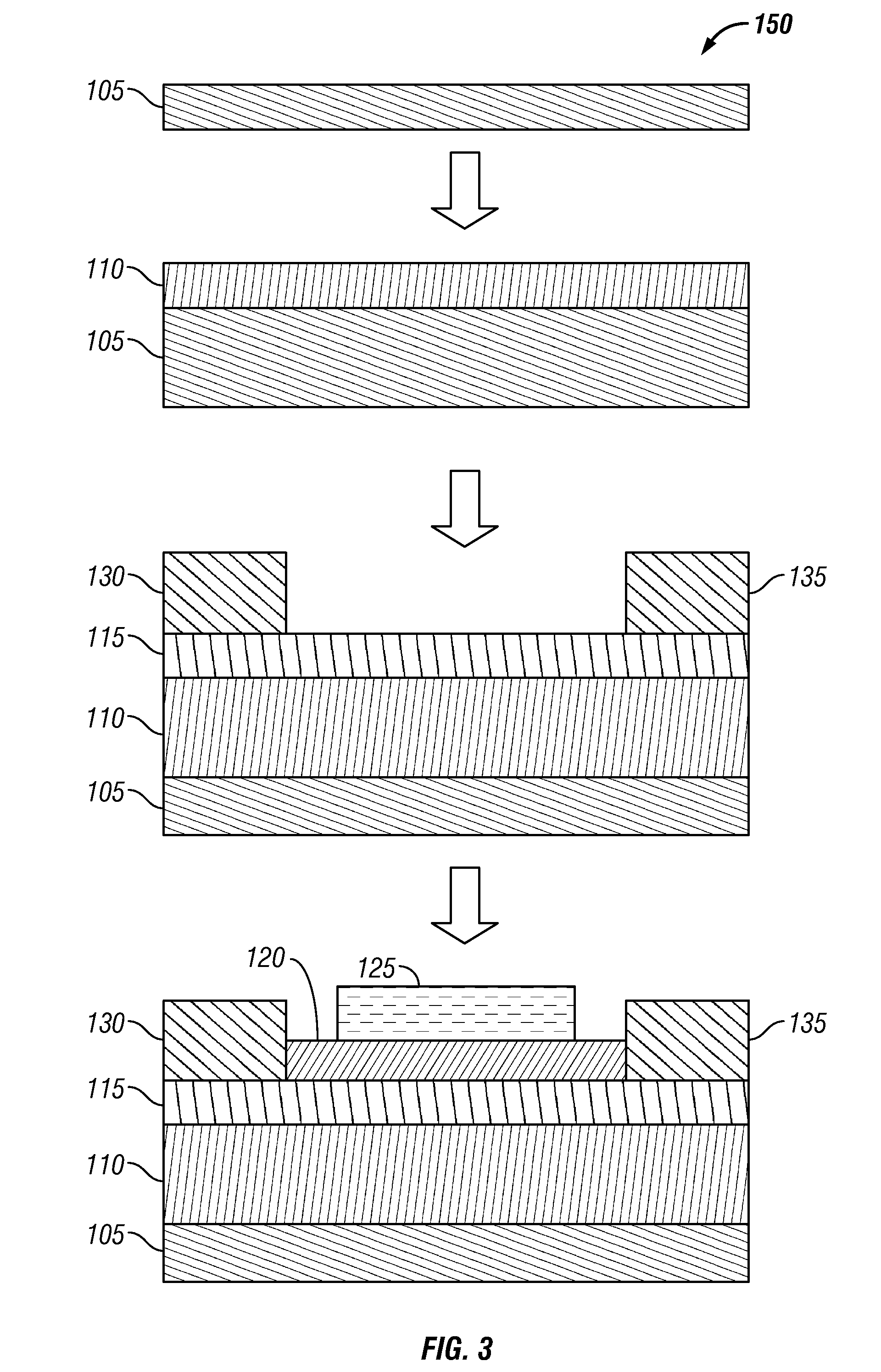
[0026]FIG. 1 illustrates a cross-sectional view of a field-effect piezoelectric strain sensor 100, in accordance with the disclosed embodiments. The field-effect piezoelectric strain sensor 100 can be mounted and subjected to a strain in order to sense force, pressure, strain, acceleration, displacement, or any other parameter of interest by suitable coupling of the parameter to generate the strain required. The sensor 100 incorporates a sequence of thin-films of piezoelectric layer 110 and semiconductor layer 115 in order to form a thin-film transistor (TFT) structure. The piezoelectric layer 110 and the semiconductor layer 115 can be deposited on a flexible substrate 105 by a low cost fabrication technique. The apparatus 100 may be, for, example, mounted on or integrally form...


PUM


Abstract

A piezoelectric strain sensor and method thereof for detecting strain, vibration, and / or pressure. The sensor incorporates a sequence of piezoelectric and semiconductor layers in a thin-film transistor structure. The thin-film transistor structure can be configured on a flexible substrate via a low-cost fabrication technique. The piezoelectric layer generates an electric charge resulting in a modulation of a transistor current, which is a measure of external strain. The sensor can be formed as a single gate field-effect piezoelectric sensor and a dual gate field-effect piezoelectric sensor. The semiconductor layer can be configured from a nanowire array resulting in a metal-piezoelectric-nanowire field effect transistor. The single and dual gate field-effect piezoelectric sensor offer increased sensitivity and device control due to the presence of the piezoelectric layer in the transistor structure and low cost manufacturability on large area flexible substrates.

Description

CROSS-REFERENCE TO PROVISIONAL APPLICATION[0001]This application claims the benefit of priority based on U.S. Provisional Patent Application Ser. No. 61 / 236,788 filed Aug. 25, 2009, entitled “Thin-Film Transistor Based Piezoelectric Strain Sensor and Method.” The above-referenced provisional patent application is hereby incorporated by reference herein in its entirety.TECHNICAL FIELD[0002]Embodiments are generally related to sensor devices and components. Embodiments are also related to strain sensors that detect strain, vibration, force, and / or pressure. Embodiments are additionally related to the fabrication of strain sensors.BACKGROUND OF THE INVENTION[0003]Strain sensors are widely utilized for measuring and monitoring strain, pressure, force, and / or vibration in certain structures in order to provide inspection and flaw detection associated with such structures. Strain sensors can detect the magnitude of stress and load in various industrial and commercial applications. Example...

Claims


Application Information

Patent Timeline
Patent Type & Authority Applications(United States)
IPC IPC(8): H01L29/84H01L21/28
CPCB82Y10/00G01L1/005G01L1/16H01L29/0665H01L29/78654H01L51/055H01L29/7869H01L29/84H01L51/0048H01L51/0516H01L29/78681H10K85/221H10K10/468H10K10/481
Inventor DUMITRU, VIOREL-GEORGELCOBIANU, CORNELCOSTEA, STEFAN-DANSERBAN, BOGDAN-CATALIN
Owner HONEYWELL ROMANIA
Why Eureka
Try Eureka