

High electromagnetic transmission composite structure
- Summary
- Abstract
- Description
- Claims
- Application Information
AI Technical Summary
Benefits of technology
Problems solved by technology
Method used
Image

Examples
first embodiment
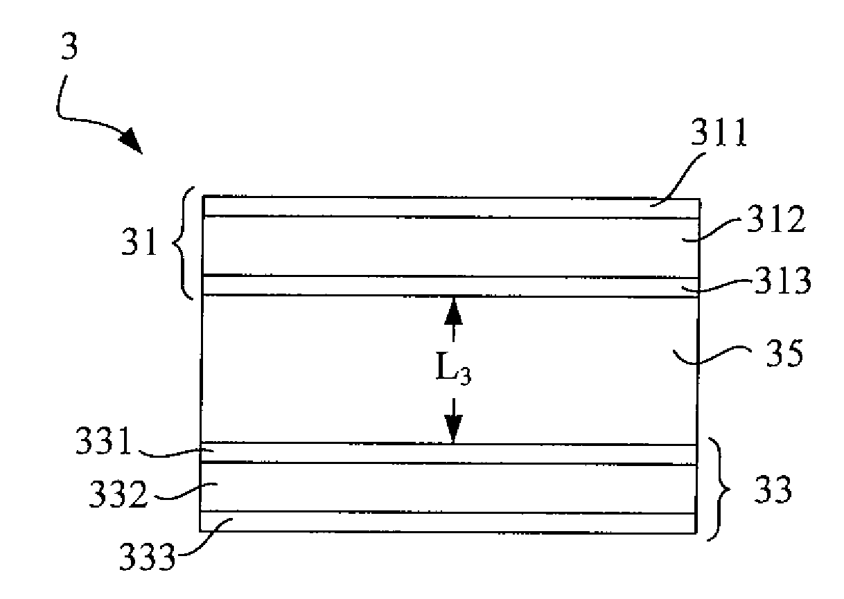
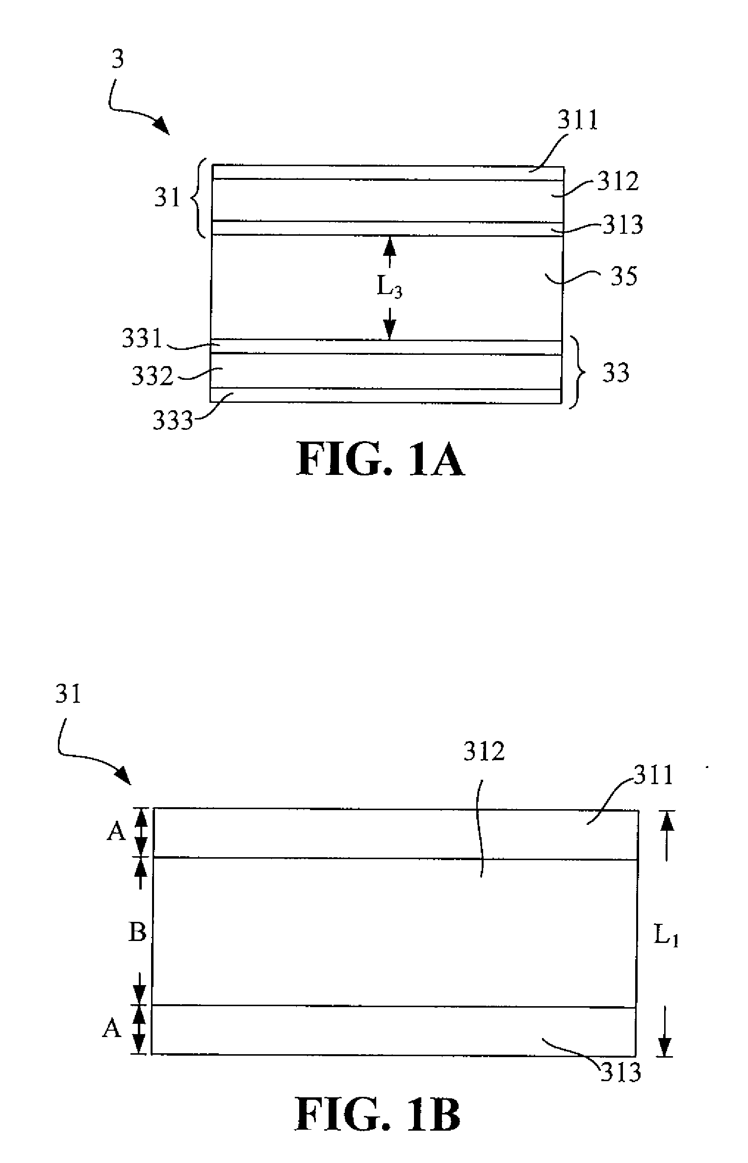
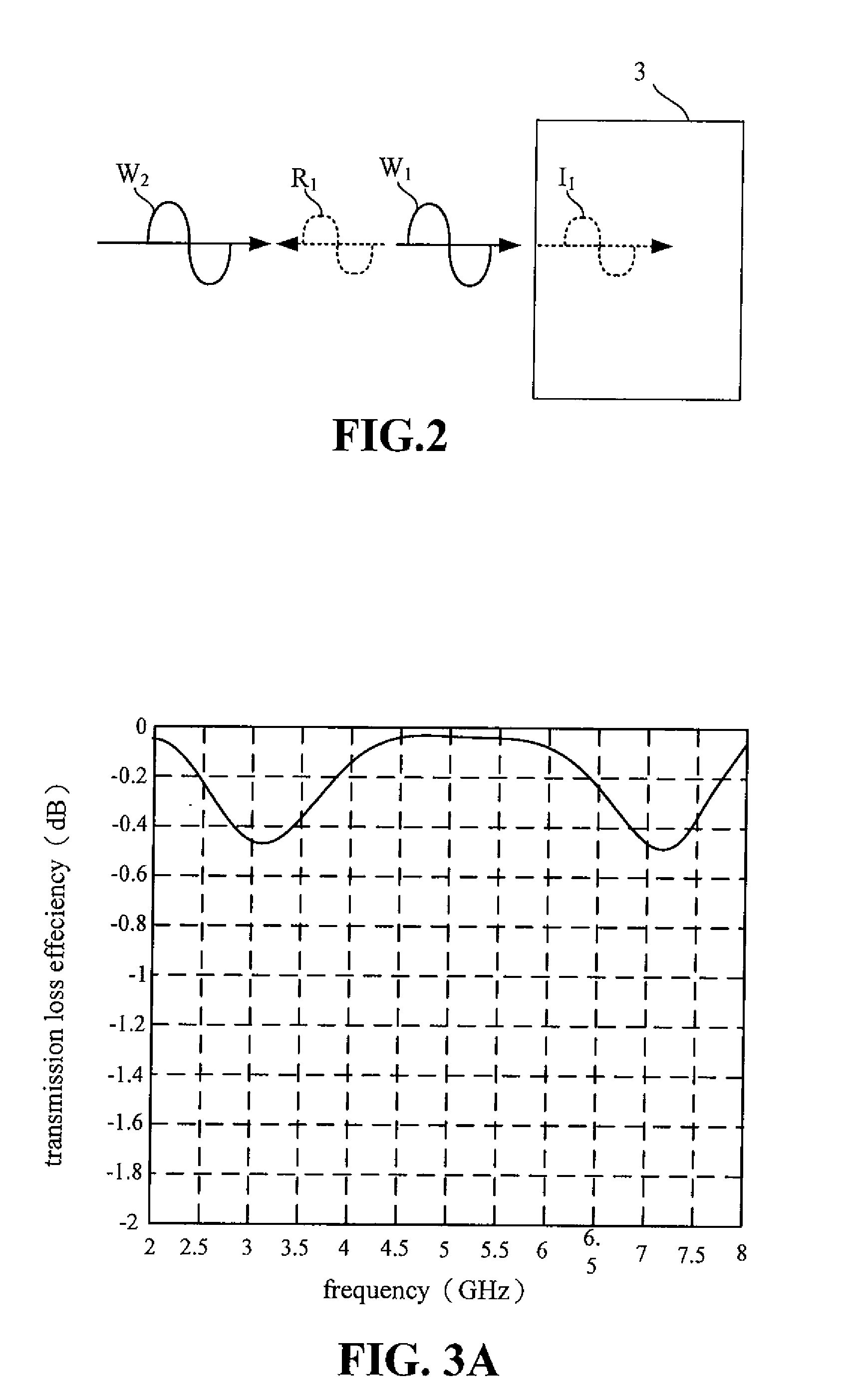
[0038]Please refer to FIG. 3A. FIG. 3A illustrates the analyzed result of the high electromagnetic transmission composite structure 3 of the invention. As shown in FIG. 3A, in the high electromagnetic transmission composite structure 3 of the invention in this embodiment, the thicknesses of the material layers are as follows: The thicknesses of the first composite board 311, the second composite board 313, the third composite board 331, and the fourth composite board 333 are all 1 mm, while the thicknesses of the first buffer layer 35, the second buffer layer 312, and the third buffer layer 332 are 30 mm, 10 mm, and 10 mm, respectively.
second embodiment
[0039]Please refer to FIG. 3B. FIG. 3B illustrates an analyzed result of the high electromagnetic transmission composite structure 3 of the invention. As shown in FIG. 3B, in the high electromagnetic transmission composite structure 3 of the invention in this embodiment, the thicknesses of the material layers are as follows: The thicknesses of the first composite board 311, the second composite board 313, the third composite board 331, and the fourth composite board 333 are all 1 mm, while the thicknesses of the first buffer layer 35, the second buffer layer 312, and the third buffer layer 332 are 45 mm, 10 mm, and 10 mm, respectively.
third embodiment
[0040]Please refer to FIG. 3C. FIG. 3C illustrates an analyzed result of the high electromagnetic transmission composite structure 3 of the invention. As shown in FIG. 3C, in the high electromagnetic transmission composite structure 3 of the invention in this embodiment, the thicknesses of the material layers are as follows: The thicknesses of the first composite board 311, the second composite board 313, the third composite board 331, and the fourth composite board 333 are all 1 mm, while the thicknesses of the first buffer layer 35, the second buffer layer 312, and the third buffer layer 332 are 60 mm, 10 mm, and 10 mm, respectively.
PUM
 Abstract
Description
Claims
Application Information